 Professional Flip-Chip Packaging Substrate Supplier

What is Ultra-small pitch substrate?
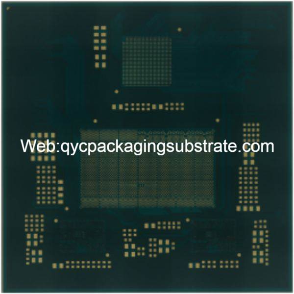
Ultra-small pitch substrate Vender: Optimal 100um bump pitch, 9um trace and gap for compact design. Typical: 15-30um trace and spacing.
Ultra-small pitch substrate is a technological innovation that has attracted much attention in the field of PCB engineering. This substrate has extremely small pin spacing and is designed in response to the trend of modern electronic devices pursuing miniaturization and high performance. Its unique design accommodates more pins in a compact space, significantly increasing the performance and functionality of electronic devices.
In the rapid evolution of today’s electronic devices, Ultra-small pitch substrate plays a vital role. Its design caters to the growing demand for miniaturization and high performance in advanced electronic devices. By using extremely small pin pitches, this substrate effectively increases the connection density between electronic devices, making it possible to accommodate more functional components in a limited space.
This substrate not only plays a key role in packaging technology, but also plays an integral role in the development of integrated circuits (ICs). Ultra-small pitch substrate is closely related to IC packaging and provides a compact base for different chip packaging technologies such as Ball Grid Array and Chip Scale Package, thereby enabling higher pin density and more compact designs.
There are various types of Ultra-small pitch substrates, including improved HDI manufacturing technology and semi-additive methods. These different types allow Ultra-small pitch substrate to adapt to different application scenarios and provide customized solutions for various electronic devices.
Compared with traditional printed circuit boards (PCBs), Ultra-small pitch substrates have significant advantages in space utilization efficiency and performance. Traditional PCBs are often limited by pitch and density, while Ultra-small pitch substrate circumvents these limitations through its miniaturized design, providing more innovative possibilities for electronic devices.
In the manufacture of Ultra-small pitch substrate, a complex multi-layer structure is used, including different metal layers and insulating layers. Its manufacturing technology involves advanced printing and stacking processes, including improved HDI manufacturing technology and semi-additive methods to achieve smaller pitches and higher density. Although there are certain challenges in the manufacturing process, the performance and application value of this substrate make it a breakthrough technology in the field of electronic engineering.
In general, the emergence of Ultra-small pitch substrate not only promotes the miniaturization and high performance of electronic devices, but also provides PCB engineers with more innovative possibilities. Through continuous improvements in manufacturing technology and structural design, Ultra-small pitch substrate will continue to play a key role in the future development of electronic technology.
Ultra-small pitch substrate
What is the function of Ultra-small pitch substrate?
Ultra-small pitch substrate is a crucial technology in today’s electronic engineering field. Its core function is to provide highly integrated electrical connections and signal transmission for advanced electronic devices.
In addition to electrical connections, another important function of Ultra-small pitch substrate is to optimize signal transmission. Its precision design and high-density layout help reduce signal transmission delays and improve signal transmission stability and reliability. This is of significant significance for application scenarios that require fast data transmission and response, such as high-performance computing and communication equipment.
Under the trend of miniaturization and high performance, Ultra-small pitch substrate further meets the needs of advanced electronic devices by implementing more functional components on small-size substrates. Its precision design and high degree of integration provide electronic engineers with greater flexibility, allowing them to implement more powerful and complex electronic systems within limited space.
Overall, Ultra-small pitch substrate is not only a technological innovation in the field of modern electronic engineering, but also a key driving force for miniaturization and high performance of electronic devices. Its superior performance in high-density electrical connections and signal transmission makes it ideal for meeting the growing requirements of today’s electronic devices. By continuously improving manufacturing technology and structural design, Ultra-small pitch substrate will continue to play an important role in the future development of electronic technology.
What types of Ultra-small pitch substrate are there?
As a crucial element in contemporary electronic devices, ultra-small pitch substrates come in diverse types tailored to meet the demands of miniaturization and high performance across various application scenarios. These variants encompass a range of materials and structures, providing electronics engineers with a multitude of options to fine-tune their design and manufacturing processes for optimal outcomes.
First of all, improved HDI (High-Density Interconnect) manufacturing technology is an important type of Ultra-small pitch substrate. This technology enables smaller pitches and higher integration by increasing pin density and inter-layer connection capabilities. HDI technology usually uses a multi-layer stack structure in which different metal layers and insulating layers are interwoven to ensure efficient electrical connection and signal transmission. This type of Ultra-small pitch substrate is suitable for scenarios that have strict requirements on the size and performance of electronic devices, such as smartphones and portable electronic devices.
On the other hand, the semi-additive method is also a common Ultra-small pitch substrate manufacturing technology. This method uses a semi-additive process to achieve smaller spacing and higher density by adding conductive materials layer by layer.
Beyond the two primary types highlighted earlier, there exist various iterations of ultra-small pitch substrates, chosen in alignment with specific application demands and design objectives. For instance, by leveraging diverse substrate materials like polyimide or FR-4, and employing distinct manufacturing processes, engineers have the flexibility to tailor ultra-small pitch substrates to suit specific scenarios. This adaptability empowers engineers to handpick the most fitting type based on project-specific requirements, ultimately ensuring optimal performance and reliability in electronic applications.
Overall, the diversity of Ultra-small pitch substrates reflects their wide application in different fields and provides electronic engineers with room for innovation and optimized design. By selecting the appropriate type, engineers can take full advantage of the superior performance of Ultra-small pitch substrates in realizing miniaturized, high-performance electronic devices. As technology continues to evolve, it is believed that Ultra-small pitch substrate will continue to play a key role in the field of electronic engineering, driving the continuous improvement of device size and performance.
What is the relationship between Ultra-small pitch substrate and IC packaging?
Ultra-small pitch substrate, as an important technology in the field of PCB engineering, is inseparable from IC packaging in modern electronic equipment. It is closely related to IC packaging, which is mainly reflected in providing a compact base and playing a key role in different chip packaging technologies.
The design concept of Ultra-small pitch substrate aims to overcome the limitations of traditional packaging technology and provide more efficient support for integrated circuits. Its extremely small pin pitch makes it possible to accommodate more pins in a limited space, which provides greater freedom for advanced IC design. This close relationship makes Ultra-small pitch substrate an ideal choice for achieving highly integrated chip packaging.
Among different chip packaging technologies, technologies such as BGA and CSP rely on Ultra-small pitch substrate to achieve higher pin density and more compact designs. BGA uses a ball grid array structure. With the support of Ultra-small pitch substrate, more pins can be arranged on the bottom of the chip, thereby increasing the connection density.
At the same time, high pin density also provides electronic equipment with more possibilities for interfaces and function expansion, satisfying the continuous pursuit of miniaturization and high performance of modern electronic equipment.
Overall, the close relationship between Ultra-small pitch substrate and IC packaging promotes the continuous progress of integrated circuit packaging technology. By providing a compact base and supporting different packaging technologies, Ultra-small pitch substrate provides key support for the miniaturization and high performance of electronic devices, driving continuous innovation in the field of electronic engineering.
What is the difference between Ultra-small pitch substrate and traditional PCB?
Ultra-small pitch substrate (ultra-small pitch substrate) has emerged in modern electronic engineering and shows striking differences compared with traditional PCB (printed circuit board). Compared with traditional circuit boards such as traditional PWBs (printed wiring boards), ordinary PCBs, and motherboards, it has become an ideal choice for advanced electronic equipment due to its smaller pitch and higher density, providing high-performance and miniaturized equipment. Provides significant advantages.
Traditional PCBs usually use large pin spacing and relatively low density, which to a certain extent limits their application in miniaturized devices. The Ultra-small pitch substrate successfully solves this problem with its precision design and compact structure. The extremely small spacing between its pins allows more pins to be accommodated in a limited space, providing more functional components for electronic devices and achieving a high degree of integration.
Compared with traditional circuit boards such as PWBs, ordinary PCBs and motherboards, Ultra-small pitch substrate has obvious advantages in terms of space utilization efficiency and performance. Traditional PCBs are often limited and difficult to adapt to the needs of modern electronic devices for miniaturization and high performance. On the contrary, the design concept of Ultra-small pitch substrate is proposed to address these challenges. Its miniaturized pitch makes the overall structure more compact and provides a more flexible layout for electronic systems.
Ultra-small pitch substrate
In modern electronic devices, the thickness and volume of traditional PCBs may become design bottlenecks, while Ultra-small pitch substrate achieves thinner and lighter characteristics by optimizing the structure and adopting more advanced manufacturing technology. This thin and light design not only conforms to today’s pursuit of lightweight electronic products, but also helps improve heat dissipation and enhance the overall performance of the device.
In addition, Ultra-small pitch substrate is more suitable for high-density packaging technology than motherboards, providing a more compact base for integrated circuits. This allows chip packaging technologies, such as BGA and CSP, to function better and achieve higher pin density and more compact designs, providing a solid foundation for the high performance of electronic devices.
In summary, Ultra-small pitch substrate, with its unique design and manufacturing technology, exhibits smaller pitch, higher density, and thinner characteristics than traditional PCBs, making it an ideal choice to meet the needs of modern electronic equipment. . Its significant advantages in space utilization efficiency and performance provide electronic engineers with more innovative possibilities and promote the continuous progress of electronic technology.
What are the main structures and production technologies of Ultra-small pitch substrate?
The ultra-small pitch substrate stands as a critical technology in contemporary electronic engineering, with its design and manufacturing processes playing pivotal roles in achieving both miniaturization and high-density packaging. Let’s delve into a closer examination of the primary structure and production technology inherent to ultra-small pitch substrates.
The structure of Ultra-small pitch substrate usually adopts a multi-layer design, which allows more pins to be accommodated in a limited space, thus improving the performance of electronic devices. These multilayer structures include different metal and insulating layers to create a compact and efficient substrate.
In terms of manufacturing technology, Ultra-small pitch substrate uses advanced printing and stacking processes. Among them, improved HDI (High-Density Interconnect) manufacturing technology is a key part. Through this technology, smaller pin spacing can be achieved on the substrate, thereby increasing the number of pins and improving connection density. This improved manufacturing technology is critical to accommodate the demands for high levels of integration and miniaturization in modern electronic devices.
Another important manufacturing technology is the semi-additive method. This is an advanced stacking process that achieves precise control of Ultra-small pitch substrate by adding metal and insulating materials layer by layer on the surface of the substrate. This method effectively reduces possible errors during the manufacturing process and ensures the high quality and stability of the substrate.
Through these advanced manufacturing technologies, Ultra-small pitch substrates achieve smaller pitches and higher densities, making them ideal for meeting the needs of modern electronic devices. The development of this technology not only promotes the miniaturization and lightweight of electronic equipment, but also brings more advanced electronic products to various industries. In the future, with the continuous innovation of manufacturing technology, we can expect Ultra-small pitch substrate to play a more important role in electronic engineering and provide strong support for the continuous progress of technology.
Ultra-small pitch substrate FAQs
What applications is Ultra-small pitch substrate suitable for?
Ultra-small pitch substrate is specially designed for electronic devices that require high integration and miniaturization, and is widely used in mobile devices, medical equipment, communication equipment and other fields. Its ultra-fine pitch design makes it ideal for meeting the compact design needs of modern electronic equipment.
What is the difference between Ultra-small pitch substrate and traditional PCB?
Ultra-small pitch substrate has smaller pin spacing and higher density than traditional printed circuit boards. This allows it to accommodate more pins in the same size, providing more functionality for electronic systems. Compared with traditional PWBs and PCBs, Ultra-small pitch substrate has significant advantages in space utilization efficiency and performance.
What is special about the manufacturing technology of Ultra-small pitch substrate?
The manufacturing of Ultra-small pitch substrate involves highly precise printing and stacking processes, including improved HDI manufacturing technology and semi-additive methods. These technologies make it possible to achieve ultra-fine pitch and high density, but they also bring certain manufacturing challenges and require advanced equipment and process control.
How is Ultra-small pitch substrate combined with IC packaging?
Ultra-small pitch substrate is closely integrated with IC packaging to provide a compact substrate for integrated circuits. The use of different chip packaging technologies, such as BGA and CSP, can achieve higher pin density and more compact designs through Ultra-small pitch substrate, further promoting the performance and functionality of electronic devices.
What is the future development direction of Ultra-small pitch substrate?
In the future, Ultra-small pitch substrates will continue to develop in a smaller and denser direction. With the continuous demand for miniaturization and high performance of electronic devices, the manufacturing technology and design of Ultra-small pitch substrate will continue to innovate to meet the changing market needs.
By answering these frequently asked questions, we can have a more comprehensive understanding of the importance of Ultra-small pitch substrate in PCB engineering and its wide application in modern electronic equipment.
Full text overview of Ultra-small pitch substrate
Ultra-small pitch substrate (ultra-small pitch substrate), as a crucial technological innovation in the field of PCB (Printed Circuit Board, printed circuit board) engineering, provides an indispensable factor for the miniaturization and high performance of modern electronic equipment. Critical support. The continuous evolution of this field and the continuous improvement of Ultra-small pitch substrate indicate that electronic technology is ushering in a new era of development.
In the modern electronics industry, as users continue to demand device miniaturization and high performance, Ultra-small pitch substrate has emerged. Its main function is to achieve a high degree of integration of electronic components through extremely small pin spacing, thereby providing more functions in a limited space. This specially designed substrate not only improves the performance of electronic devices, but also drives a wave of technological innovation.
Different from traditional PCB, Ultra-small pitch substrate is more complex in structure and adopts a multi-layer stack design, including different metal layers and insulating layers. The highly precise processes involved in the manufacturing process, such as improved HDI manufacturing technology and semi-additive methods, allow this ultra-fine pitch substrate to maintain stability and reliability while achieving smaller pitches and higher density.
Closely related to IC packaging, Ultra-small pitch substrate provides a solid foundation for the development of integrated circuits. Using different chip packaging technologies, such as BGA (Ball Grid Array) and CSP (Chip Scale Package), Ultra-small pitch substrate can achieve higher pin density and more compact design, making electronic products better in performance and appearance. has been optimized.
In the comparison between traditional PCB and Ultra-small pitch substrate, the latter has smaller pitch and higher density, providing an ideal choice for advanced electronic devices. Standing out from traditional circuit boards such as PWBs (Printed Wiring Boards), ordinary PCBs, motherboards, etc., Ultra-small pitch substrate has significant advantages in space utilization efficiency and performance.
With the continuous upgrading of electronic equipment, the future prospects of Ultra-small pitch substrate are promising. By continuously improving manufacturing technology and structural design, this key technology will continue to play an important role in promoting the development of electronic technology. Its superiority in high integration and miniaturization will open up new possibilities for more advanced and compact electronic products in the future, further promoting the prosperity and innovation of the entire electronics industry. The rise of Ultra-small pitch substrate is not only a witness to technological progress, but also a leader in the development of the electronic field, providing a solid foundation for us to embrace the future of technology.