 Professional Flip-Chip Packaging Substrate Supplier

Ultrathin BT PCB Manufacturing. Ultrathin/extra small spacing BT LED PCBs, Ultrathin package substrates. High speed and high frequency material packaging substrate manufacturing. Advanced packaging substrate manufacturer .
In today’s electronics industry, ultra-thin Bluetooth PCB has become an indispensable core component of many innovative products. This article will lead you to deeply explore the manufacturing process of ultra-thin Bluetooth PCB, and fully understand its design principles, manufacturing processes, costs and other key information. Through the guidance of this article, you will be able to better understand the important role of ultra-thin Bluetooth PCB in modern electronic products, and how to effectively design and manufacture high-performance ultra-thin Bluetooth PCB.
What is an ultra-thin Bluetooth PCB?
Ultra-thin Bluetooth PCB (Printed Circuit Board) is a PCB specially designed to support wireless communication with Bluetooth technology. With the popularity of mobile devices and smart home products, the demand for thinner, more compact electronic products continues to increase, and ultra-thin Bluetooth PCBs have emerged.
First of all, ultra-thin Bluetooth PCB is known for its extremely thin thickness. Traditional PCBs are usually thicker, but ultra-thin Bluetooth PCBs minimize their thickness by using highly optimized materials and processes. This makes it ideal for designing thinner, lighter products. Whether it is smart watches, headphones, smart glasses or other portable devices, ultra-thin Bluetooth PCB can provide greater design flexibility and space utilization.
Secondly, ultra-thin Bluetooth PCB is highly integrated. In a limited space, it integrates various necessary circuits and components, including Bluetooth chips, antennas, sensors, etc., achieving a high degree of functional integration and performance optimization. This high degree of integration makes product design simpler and more refined, while improving product performance and reliability.
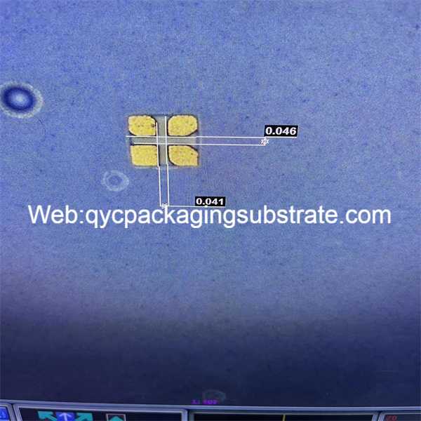
Ultrathin BT PCB manufacturing
Ultra-thin Bluetooth PCB is widely used in various consumer electronics and smart devices. For example, Bluetooth connections in smartphones and tablets, smart wearable devices, smart home products, etc. They provide stable wireless connections for these products, enabling data transmission and interconnection between devices.
In short, ultra-thin Bluetooth PCB plays a vital role in the design and manufacturing of thin and light products due to its extremely thin thickness and high integration. With the continuous development and popularization of wireless technology, ultra-thin Bluetooth PCB will continue to play an important role in the innovation and development of electronic products.
How to design ultra-thin Bluetooth PCB?
Designing an ultra-thin Bluetooth PCB is a complex and critical task that requires multiple factors to be considered to ensure the performance and reliability of the final product. Here are a few key factors to consider when designing an ultra-thin Bluetooth PCB:
The thickness of ultra-thin PCBs is usually between tens to hundreds of microns, so special attention needs to be paid to material selection and stacking structure during the design process. Choosing substrates and conductive layers with appropriate thickness can effectively reduce the overall thickness of the PCB while ensuring signal transmission and thermal management performance.
Wiring is a crucial part of PCB design, especially for ultra-thin PCBs. During the design process, the layout of signal lines, power lines, and ground lines needs to be properly planned to minimize signal interference and electromagnetic interference. Using appropriate line width and spacing and avoiding too dense wiring can effectively improve the stability and reliability of PCB.
In the design of ultra-thin PCBs, power management is a crucial consideration. Designers need to ensure power line stability and efficiency while minimizing power consumption and heat generation. Using appropriate power management chips and capacitors can effectively improve PCB power consumption efficiency and battery life.
In order to efficiently design ultra-thin Bluetooth PCB, CAD (Computer-Aided Design) software is usually used for design. These software provide a wealth of tools and functions that can help designers optimize layout and circuit routing, while performing simulation and verification to ensure PCB performance and reliability. Through CAD software, designers can quickly generate PCB layout diagrams and schematics, and perform multi-layer wiring and signal simulation to meet product design requirements.
Designing ultra-thin Bluetooth PCB requires designers to comprehensively consider thickness, wiring, power management, etc. to ensure the performance and reliability of the final product. By rationally selecting materials, optimizing layout and circuit directions, and using CAD software for design and simulation, the design efficiency and quality of ultra-thin PCBs can be effectively improved to meet the needs of different application scenarios.
What is the manufacturing process of ultra-thin Bluetooth PCB?
The process of manufacturing ultra-thin Bluetooth PCB is similar to traditional PCB, but some steps require special processes and materials. The manufacturing process of ultra-thin Bluetooth PCB will be introduced in detail below:
First, high-quality substrate and conductive layer materials need to be prepared. For ultra-thin PCBs, commonly used base materials include polyimide (PI) and polytetrafluoroethylene (PTFE), while the conductive layer usually uses copper foil or other highly conductive materials.
At the beginning of the manufacturing process, the substrate is draped over the coater. With coating, a protective covering is applied to the surface of the substrate to prevent corrosion and damage in subsequent process steps.
After coating is completed, the PCB board will be covered with a mask with a design pattern. Next, the PCB is exposed to UV light so that the light hits the mask. This way, the unexposed portions of the mask will remain to form the circuit pattern.
After the exposure is completed, place the PCB board into the etching tank. The chemical solution in the etching bath will etch away the unexposed parts of the mask, exposing the substrate surface. This step allows the unnecessary parts to be etched away to form a circuit pattern.
After you complete the circuit pattern, you need to drill holes. The location and size of the drilled holes need to be precisely controlled to ensure accurate connections to other components.
The last step is electroplating. Through electroplating, a layer of metal is covered on the surface of the PCB board to enhance its conductive properties and protect its surface from corrosion. Electroplating can also improve the welding performance and corrosion resistance of PCB boards.
Overall, the process of manufacturing ultra-thin Bluetooth PCB requires strict quality control and precision operations. Special processes and materials ensure that the ultra-thin characteristics of PCB are maintained, while also ensuring the performance and reliability of electronic products.
How much does an ultra-thin Bluetooth PCB cost?
The cost of ultra-thin Bluetooth PCB is a complex and critical issue, which is affected by many factors. Before understanding these factors, let us first sort out the characteristics of ultra-thin Bluetooth PCB. Compared with traditional PCBs, ultra-thin Bluetooth PCBs have higher integration and thinner thickness, so they require higher technical requirements in design and manufacturing. This also results in relatively high manufacturing costs.
First of all, material is one of the important factors affecting the cost of ultra-thin Bluetooth PCB. Since ultra-thin PCB requires the use of special high-performance materials, such as polyimide (PI) or polytetrafluoroethylene (PTFE), the cost of these materials themselves is relatively high. Moreover, in the manufacturing process of ultra-thin PCBs, the quality and performance requirements of materials are also more stringent, so choosing the right materials is crucial to cost control.
Secondly, the process is also one of the important factors affecting the cost of ultra-thin Bluetooth PCB. Since the manufacturing of ultra-thin PCB requires higher-precision processing equipment and process technology, the manufacturing cost is relatively high. For example, the etching and drilling processes of ultra-thin PCBs require higher precision and stability, which require more investment to ensure quality and stability.
In addition, size and quantity will also have an impact on the cost of ultra-thin Bluetooth PCBs. Generally speaking, larger sizes and smaller quantities of ultra-thin PCBs will incur higher costs because they increase material waste and production costs. Mass production can reduce the cost of unit PCB because the proportion of fixed costs can be reduced by optimizing the production process and improving efficiency.
In general, although the manufacturing cost of ultra-thin Bluetooth PCB is relatively high, the cost can be reduced by optimizing the design, selecting appropriate materials and processes, and mass production. For customers, understanding these factors and choosing the right manufacturer to cooperate can reduce costs while ensuring quality, thereby achieving better product cost performance.
What is the material of ultra-thin Bluetooth PCB?
The material of ultra-thin Bluetooth PCB is one of the key factors to ensure its performance and reliability. Since ultra-thin PCBs usually need to carry complex circuit designs and high-frequency signal transmission, choosing the right material is crucial to ensure their stable operation.
FR-4 is one of the most commonly used PCB substrates, and its excellent electrical and mechanical properties make it the first choice for many electronic devices. FR-4 has good insulation properties and can effectively prevent short circuits between circuit boards. Its high temperature resistance also makes it suitable for various working environments. For ultra-thin Bluetooth PCBs, the advantage of FR-4 is its stable size and cost-effectiveness, which can meet the requirements of most applications.
Polyimide is a material with extremely high temperature stability and mechanical strength, and is often used in electronic devices that require high performance. Its advantages include excellent high temperature resistance, chemical corrosion resistance and insulation properties, and is suitable for high frequency and high speed signal transmission occasions. For ultra-thin Bluetooth PCBs, polyimide can provide better thermal management and more stable signal transmission, and is suitable for some scenarios with higher performance requirements.
PTFE is a material with excellent electrical properties and chemical stability that is commonly used in the manufacture of high-frequency and microwave circuits. Its low dielectric constant and low loss tangent give it excellent performance in high-frequency signal transmission. For ultra-thin Bluetooth PCB, PTFE can provide better signal fidelity and anti-interference capabilities, and is suitable for application scenarios requiring high frequency and high-speed transmission.
To sum up, ultra-thin Bluetooth PCBs usually use high-performance materials such as FR-4, polyimide, and PTFE. Selecting the appropriate material depends on the requirements of the specific application and requires comprehensive consideration of factors such as circuit design, operating environment, and performance requirements. By selecting appropriate materials, you can ensure that ultra-thin Bluetooth PCB can operate stably and reliably in various application scenarios.
Who makes ultra-thin Bluetooth PCBs?
Manufacturers who manufacture ultra-thin Bluetooth PCBs usually need advanced production equipment and rich experience. In today’s highly competitive electronics market, choosing a reliable manufacturer is crucial to ensuring product quality and meeting delivery lead times. At our company, we provide high-quality ultra-thin Bluetooth PCB manufacturing services to our customers to meet their needs.
First, we have advanced production equipment and technical teams that can achieve high-precision PCB manufacturing. We use the latest production processes and quality control standards to ensure that each PCB meets our customers’ requirements and specifications. Our production lines include automated equipment and precision machining tools that can meet a variety of complex PCB manufacturing needs.
Secondly, we have rich experience and expertise to provide customers with customized solutions. No matter what the customer’s needs are, we can flexibly adjust and optimize according to their requirements to ensure the performance and reliability of the final product. Our engineering team has many years of experience in PCB design and manufacturing and can provide customers with professional technical support and consulting services.
Most importantly, we are committed to building long-term relationships and ensuring customer satisfaction. We focus on communication and cooperation with customers, and always pay attention to customer needs and feedback. We not only provide customers with high-quality products, but also provide timely after-sales support and maintenance services to ensure that customers’ interests are maximized.
To sum up, choosing a reliable manufacturer is crucial to ensuring the quality and delivery time of ultra-thin Bluetooth PCB. At our company, we have advanced production equipment, rich experience and a professional team to provide customers with high-quality PCB manufacturing services. We look forward to working with you and providing support and assistance with your projects.
Five Characteristics of Great Customer Service
Excellent customer service is crucial for ultra-thin Bluetooth PCB manufacturers. In a highly competitive market environment, good customer service can not only meet customer needs, but also enhance customer trust and loyalty to the brand. Here are five quality customer service characteristics an ultra-thin Bluetooth PCB manufacturer should have:
First of all, it is very important to provide immediate technical support and consulting services. Customers may encounter various technical problems during PCB design or production and need timely solutions and suggestions. Therefore, manufacturers should establish a professional technical support team that can quickly respond to customer inquiries and provide effective solutions.
Secondly, provide customized solutions to meet customer needs. Different customers may have different needs and requirements, and manufacturers should flexibly adjust the production process to tailor-make ultra-thin Bluetooth PCB products that meet their needs. By working closely with customers, manufacturers can better understand their needs and provide more satisfactory solutions.
Third, ensure production quality and delivery cycle. When customers choose a PCB manufacturer, what they care most about is product quality and delivery time. Therefore, manufacturers must strictly control the production process to ensure that products meet customer quality standards and are delivered on time. When facing problems, manufacturers should take timely corrective measures to ensure product quality and delivery cycle.
Fourth, provide after-sales support and maintenance services. Customers may encounter various problems when using ultra-thin Bluetooth PCB products, requiring manufacturers to provide timely after-sales support and maintenance services. Manufacturers should establish a complete after-sales service system that can quickly respond to customer problems and provide effective solutions to ensure normal use and satisfaction of customers.
Finally, maintain close communication with customers and establish long-term cooperative relationships. Manufacturers should establish a good communication mechanism with customers and regularly communicate with customers about product needs, progress and feedback. By establishing long-term relationships, manufacturers can better understand customers’ needs and expectations, and continuously improve products and services to increase customer satisfaction and loyalty.
In conclusion, excellent customer service is the key to success for ultra-thin Bluetooth PCB manufacturers. By providing immediate technical support and consulting services, customized solutions, ensuring production quality and delivery lead time, providing after-sales support and maintenance services, and maintaining close communication with customers, manufacturers can win the trust and support of customers and maintain a competitive advantage. and achieve long-term development.
FAQS
What is the optimal thickness for an ultrathin BT PCB?
The optimal thickness for an ultrathin BT (Bluetooth) PCB depends on various factors such as the specific application, mechanical requirements, and manufacturing capabilities. Generally, ultrathin BT PCBs have thicknesses ranging from 0.2mm to 0.8mm. However, the optimal thickness may vary depending on factors like signal integrity, thermal management, and mechanical stability. Designers often need to balance these factors to determine the most suitable thickness for their application.
How many layers of routing can ultrathin BT PCB support?
The number of routing layers that ultrathin BT PCBs can support depends on the complexity of the design and the manufacturing process capabilities. Typically, ultrathin BT PCBs can accommodate multiple routing layers, ranging from two to ten or more layers. However, increasing the number of routing layers may pose challenges in terms of signal integrity, manufacturing cost, and board thickness. Designers need to carefully consider these factors and work closely with PCB manufacturers to determine the optimal number of routing layers for their specific application.
How to choose the suitable material for ultrathin BT PCBs?
Choosing the suitable material for ultrathin BT PCBs is crucial to ensure reliable performance and durability. Common materials used for ultrathin BT PCBs include flexible substrates such as polyimide (PI) and liquid crystal polymer (LCP), which offer excellent flexibility and thermal stability. Additionally, high-performance rigid materials like FR-4 and Rogers materials are also used for ultrathin BT PCBs to provide enhanced signal integrity and mechanical strength. When selecting materials for ultrathin BT PCBs, designers need to consider factors such as electrical properties, mechanical properties, thermal performance, and cost to meet the specific requirements of their application.
What is the optimal thickness for ultrathin BT PCBs?
The optimal thickness for ultrathin BT PCBs typically depends on the specific requirements of the application and the desired level of flexibility. However, in general, ultrathin PCBs for Bluetooth devices often range from 0.2mm to 0.8mm in thickness. This range allows for a balance between mechanical flexibility and electrical performance.
How many layers of routing can ultrathin BT PCBs support?
Ultrathin BT PCBs can support varying numbers of routing layers depending on the complexity of the circuit design and the manufacturing capabilities of the chosen PCB manufacturer. While some ultrathin PCBs may only have two layers for simple designs, others can accommodate up to eight or more layers for more intricate circuits.