 Professional Flip-Chip Packaging Substrate Supplier

Ultrathin PCB manufacturing, we mainly produce ultra-small bump pitch substrate, ultra-small trace and spacing packaging substrate and PCBs.
What is ultra-thin PCB?
Ultra-thin PCB (Printed Circuit Board) is a printed circuit board specially designed for extremely compact electronic devices. Its thickness is usually less than 0.4 mm of traditional PCB. These ultra-thin PCBs often use advanced materials and manufacturing processes to achieve greater flexibility and performance. Compared with traditional PCBs, ultra-thin PCBs are widely used in electronic products, including smartphones, wearable devices, medical implants, etc.
Ultra-thin PCBs differ from traditional PCBs in several ways. First, the thickness of ultra-thin PCBs is significantly reduced, which allows them to fit into more compact device designs. Secondly, ultra-thin PCBs usually use flexible substrate materials, such as polyimide (PI) or liquid crystal polymer (LCP), which have excellent flexibility and high temperature resistance, making the PCB less likely to break when bent or stressed. In addition, the design and manufacturing process of ultra-thin PCBs may also be slightly different from traditional PCBs, requiring greater precision and specialized equipment.
The emergence of ultra-thin PCBs has enriched the design possibilities of electronic devices. They provide product designers with more space and flexibility, allowing them to develop thinner, lighter and more portable products. At the same time, ultra-thin PCB also provides higher performance and reliability, ensuring stable operation of equipment in extreme environments.
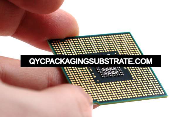
Ultrathin PCB manufacturing
In general, ultra-thin PCBs are an indispensable component of modern electronic equipment. Their emergence has brought new possibilities to the development of electronic products and promoted the continuous progress and innovation of technology.
How to design ultra-thin PCB?
Designing ultra-thin PCBs is a complex and delicate task that requires consideration of multiple factors to ensure design accuracy and performance. Here are the key factors to consider when designing ultra-thin PCBs:
Choosing the right substrate material is critical. For ultra-thin PCBs, commonly used materials include polyimide (PI) and liquid crystal polymer (LCP), which are favored for their high flexibility and thermal stability.
In the design of ultra-thin PCBs, the design of the stack-up structure is crucial. Proper stack-up design can improve the mechanical stability and electrical performance of the board while minimizing the thickness of the board.
During the design process of ultra-thin PCBs, component layout needs to be optimized to minimize the thickness of the board. Proper component layout not only saves space, but also improves circuit performance and reliability.
When designing ultra-thin PCBs, wire paths need to be carefully designed to ensure they are detailed and dense enough to minimize the thickness of the board and ensure the stability and reliability of the circuit.
Ultra-thin PCBs often face more stringent thermal management challenges. Therefore, thermal dissipation paths need to be considered during the design process to ensure that circuit components maintain stable temperatures while operating.
Since the design of ultra-thin PCBs usually requires high mechanical strength of the board, the stability and strength of the structure need to be considered in the design to ensure that the PCB will not be deformed or damaged during use.
In order to ensure signal stability and anti-interference ability, the design of ultra-thin PCB usually requires separating analog and digital signals and taking corresponding shielding measures.
After the design is completed, rigorous testing and verification must be performed to ensure that the ultra-thin PCB design meets expected performance specifications and meets customer needs and standards.
When designing ultra-thin PCBs, it is necessary to consider the above factors and utilize advanced design tools and techniques to ensure the accuracy, reliability and performance of the final design. By deeply understanding the design requirements of ultra-thin PCBs, we can provide more innovative possibilities for the development of modern electronic products.
What is the manufacturing process for ultra-thin PCBs?
The manufacturing process of ultra-thin PCB is a precise and complex process involving multiple key steps, each of which is crucial and affects the quality and performance of the final product. Here are the main steps in ultra-thin PCB manufacturing and how to ensure quality and stability:
Material preparation: The first step in manufacturing ultra-thin PCB is to prepare the materials. Choosing the right substrate material is critical, and common choices include polyimide (PI) and liquid crystal polymer (LCP). These materials have good flexibility and heat resistance and are suitable for ultra-thin PCB applications.
Graphics Image Transfer (GIP): GIP is a critical step in transferring the design image to the substrate. This is usually achieved through photolithography or direct printing techniques. Precise graphics image transmission ensures the accuracy and clarity of circuit patterns.
Copper foil deposition: Copper foil is deposited on the surface of the substrate to form a conductive layer. Uniform deposition and proper thickness of copper foil are critical to PCB performance. Precise control of copper foil thickness ensures the stability and conductivity of the circuit.
Photolithography and etching: Use photolithography technology to expose the circuit pattern on the surface of the copper foil, and use chemical etching to remove the unexposed copper foil. This step determines the shape and structure of the circuit and requires high-precision process control to ensure the clarity and consistency of the circuit pattern.
Hole Drilling: Using laser drilling or mechanical drilling techniques to create holes in a PCB to connect circuits between different layers. The exact location and size of holes is critical to PCB performance and reliability.
Metallization and surface treatment: A metallization layer is applied to the surface of the PCB, usually using processes such as gold plating or tin plating. This step is designed to improve welding reliability and corrosion resistance, ensuring the stability and durability of the circuit connection.
Printing and SMT: Print logos and text information on PCBs and accurately mount electronic components. Proper printing and placement processes ensure circuit marking clarity and component robustness.
Final Inspection and Testing: After completing PCB manufacturing, final inspection and testing is performed. This includes visual inspection, electrical testing, functional testing, etc. to ensure that the PCB meets the design requirements and has good performance and reliability.
By strictly controlling the quality and precision of each manufacturing step and employing advanced process technology and equipment, manufacturers are able to ensure the quality and stability of ultra-thin PCBs to meet customer needs and expectations.
How to make ultra-thin PCB?
Manufacturing ultra-thin PCBs is a precise and complex process that requires special equipment and advanced technology. Here are the key steps in manufacturing ultra-thin PCBs and ways to ensure the accuracy and efficiency of the manufacturing process.
Precision Cutting Machine: The fabrication of ultra-thin PCBs requires cutting the substrate material to precise dimensions. Precision cutting machines can achieve high-precision cutting to ensure that the size of the plate meets the design requirements.
High-resolution developing equipment: The developing process in PCB manufacturing is especially critical for ultra-thin PCBs. High-resolution developing equipment can accurately control the concentration and time of the developer to ensure that fine circuit structures are clearly developed and ensure the reliability of the circuit.
Miniaturized gold plating equipment: The metallization process of ultra-thin PCB requires miniaturized gold plating equipment. These devices enable uniform metal deposition in extremely small spaces, ensuring circuit conductivity and stability.
Strict process control: Manufacturing ultra-thin PCBs requires strict control of the parameters of each process step. From substrate pretreatment to circuit printing to metallization, each step requires precise control of temperature, time and chemical concentration to ensure product quality and stability.
Advanced automation technology: Manufacturing ultra-thin PCBs requires highly automated production lines. Advanced automation equipment improves production efficiency, reduces human error, and ensures consistent quality for every PCB.
Strict quality control: Strict quality control measures need to be implemented during the manufacturing process. By using advanced testing equipment and technology, defects in the production process are discovered and corrected in a timely manner to ensure that the final product meets customer requirements and industry standards.
Through the above special equipment and carefully designed manufacturing processes, the accuracy and efficiency of manufacturing ultra-thin PCBs are ensured. The application of these technologies and methods provides reliable guarantee for the manufacturing of ultra-thin PCBs and promotes the development of electronic products towards thinner, lighter and higher performance.
How much does an ultra-thin PCB cost?
The cost of ultra-thin PCBs is a complex issue that is influenced by many factors. Compared with traditional PCBs, the manufacturing of ultra-thin PCBs requires more investment in technology and resources, and therefore generally costs more. The following are the key factors that influence the cost of ultra-thin PCBs:
Material Cost: The materials used in ultra-thin PCBs are generally more expensive than traditional PCBs. For example, special substrate materials (such as polyimide or liquid crystal polymer) and high-precision copper foil for ultra-thin PCBs may increase manufacturing costs.
Manufacturing complexity: The manufacturing process of ultra-thin PCB is more complex than traditional PCB and requires higher-precision equipment and technology. For example, to ensure the quality and stability of ultra-thin PCBs, special processing techniques and sophisticated control systems may be required, which increases manufacturing costs.
Design requirements: The design of ultra-thin PCBs often requires more engineers and design time to optimize layout, routing and stack-up structures. Complex design requirements may result in increased design costs.
Throughput: The cost of manufacturing ultra-thin PCBs is also affected by throughput. Typically, high-volume production reduces average manufacturing costs, while low-volume production may increase costs.
Technical requirements: The manufacturing of ultra-thin PCB requires high-precision technology and equipment to ensure precise control of parameters such as board thickness and line width. These technical requirements may increase manufacturing costs.
In comparison, ultra-thin PCBs typically cost more than traditional PCBs. This is mainly because ultra-thin PCBs require the use of more expensive materials, more complex manufacturing processes, and more labor and technology investment. However, with the development of technology and the increase in market demand, the cost of ultra-thin PCBs is gradually declining, making it possible to adopt more application scenarios.
Manufacturing cost is an important consideration when deciding whether to use ultra-thin PCBs. Businesses need to consider design requirements, technical feasibility and budget constraints to select the PCB type that best suits their needs and balances cost with performance.
By gaining a deeper understanding of the cost structure and influencing factors of ultra-thin PCBs, companies can better plan and manage their product development and manufacturing processes to become more competitive and meet customer needs.
What materials are ultra-thin PCBs made of?
Material selection for ultra-thin PCBs is critical because they directly affect the board’s flexibility, thermal conductivity, and electrical performance. Below we will explore what materials ultra-thin PCBs are mainly composed of and their characteristics.
The substrate of ultra-thin PCB usually uses high-performance plastics such as polyimide (PI) or liquid crystal polymer (LCP) as the base material. These materials have excellent heat resistance, chemical stability and mechanical strength, allowing ultra-thin PCBs to work in a variety of extreme environments and have excellent resistance to deformation.
As the core component of PCB, copper foil is usually used as the conductive layer. In ultra-thin PCBs, the thickness of the copper foil is usually relatively thin to ensure flexibility and lightweight of the board. In addition, the good conductive properties of copper foil also help improve the performance and stability of the circuit.
Insulating layers play a key role in ultra-thin PCBs, isolating conductive layers and preventing short circuits between circuits. Common insulation materials include polyimide film (PI), polyester film, polytetrafluoroethylene (PTFE), etc., which have excellent insulation properties and chemical stability.
Soldering pads are key components used to connect electronic components and are usually made of metallic materials such as tin-lead alloy or lead-free solder. In ultra-thin PCBs, the pads are designed taking into account the flexibility and thinness of the board to ensure soldering quality and reliability.
The solder mask is designed to protect the PCB surface and prevent the conductive layer from contacting the external environment. Common solder mask materials include epoxies and polyurethanes, which offer good heat and corrosion resistance while also providing additional mechanical protection.
In general, the material selection for ultra-thin PCB needs to comprehensively consider factors such as circuit performance, structural strength, and manufacturing process. Through reasonable selection of materials and precision processing, ultra-thin PCBs with excellent performance and compact structure can be produced to meet the needs of modern electronic equipment for thinness, lightness and high performance.
Who makes ultra-thin PCBs?
The manufacturing of ultra-thin PCBs is a precise and complex process that requires highly specialized equipment and technology. In the field of ultra-thin PCB manufacturing, supplier selection is crucial because they not only affect product quality, but also directly impact customer satisfaction and project progress. As a professional electronics manufacturing company, we are actively involved in the manufacturing of ultra-thin PCBs and have won the trust of our customers with our excellent technology and services.
Our manufacturing facility is equipped with advanced production lines and equipment specifically for the production of ultra-thin PCBs. From high-precision material processing to complex molding processes, we strictly follow industry standards and continuously optimize the production process to ensure product quality and production efficiency reach the best level.
In addition to equipment and technology, we have an experienced and efficient team with rich experience and expertise in the field of ultra-thin PCB manufacturing. Not only can they accurately grasp customer needs, they can also promptly solve various challenges in production to ensure that projects proceed smoothly and are delivered on time.
As one of the leaders in ultra-thin PCB manufacturing, we are committed to providing our customers with comprehensive service and support. Whether it is technical consultation, sample production or mass production needs, we are able to meet our customers’ various needs and provide customized solutions.
Overall, as a professional ultra-thin PCB manufacturer, we have won market recognition with excellent quality, reliable delivery and excellent customer service. We will continue to be committed to technological innovation and service optimization, and work hand in hand with customers to jointly promote the development of the ultra-thin PCB manufacturing industry.
What are the key attributes of good ultra-thin PCB customer service?
What are the key attributes of good ultra-thin PCB customer service? This is a crucial question because excellent customer service not only increases customer satisfaction, but also enhances a company’s reputation and competitiveness. Here are the key attributes of quality ultra-thin PCB customer service:
Professional knowledge and technical support: A high-quality ultra-thin PCB manufacturer should have rich professional knowledge and technical strength and be able to provide customers with accurate technical support and solutions. They should understand every aspect of ultra-thin PCB manufacturing and be able to help customers understand the design and features of the product.
Customized services: Customer needs vary, and a high-quality ultra-thin PCB manufacturer should be able to flexibly meet customers’ customized needs. Whether it’s a special design requirement or an urgent delivery time, they should be able to provide customers with personalized solutions.
Transparent communication: High-quality ultra-thin PCB manufacturers should establish a transparent communication mechanism with customers and provide timely feedback to customers on production progress, quality control conditions, and possible delays or problems. Through positive communication, customers’ trust and satisfaction with the company can be enhanced.
Quality Control and Assurance: High-quality ultra-thin PCB manufacturers should strictly implement quality control standards to ensure product stability and reliability. They should use advanced testing equipment and technology to conduct comprehensive inspection and testing of each batch of products to ensure that they meet customer requirements and expectations.
After-Sales Service and Support: A quality ultra-thin PCB manufacturer should provide ongoing after-sales service and support to its customers. Whether it is technical problems in product use or subsequent maintenance needs, they should be able to respond promptly and provide effective solutions to ensure continued customer satisfaction.
How to ensure customer satisfaction and product quality? This is the direction that high-quality ultra-thin PCB manufacturers need to continuously strive for. They can continuously improve customer satisfaction and product quality levels by establishing a complete quality management system, continuously improving production processes and technical levels, strengthening communication and cooperation with customers, and continuously improving the professionalism and service awareness of employees. Only in the process of continuous pursuit of excellence can high-quality ultra-thin PCB manufacturers remain invincible in the fierce market competition and win the trust and support of customers.
Frequently Asked Questions
What are the applicable scopes of ultra-thin PCB?
Ultra-thin PCBs are mainly used in compact electronic devices such as smartphones, wearable devices, medical implants, etc. Due to its thinness and lightweight characteristics, ultra-thin PCB has broad application prospects in these fields.
How to ensure the stability and reliability of ultra-thin PCBs?
Ensuring the stability and reliability of ultra-thin PCBs requires high-quality materials, precision design and rigorous production processes. In addition, adequate testing and quality control are also key to ensuring product quality.
What are some common problems you may encounter in ultra-thin PCB manufacturing?
Common problems that may be encountered in ultra-thin PCB manufacturing include material deformation, circuit shorts, excessive wiring density, etc. These problems need to be discovered in time and corresponding measures must be taken to solve them to ensure product quality and production efficiency.
How environmentally friendly are ultra-thin PCBs?
The environmental friendliness of ultra-thin PCBs depends on the materials and production processes used. Some manufacturers use environmentally friendly materials and processes, such as lead-free soldering and scrap recycling, to reduce their impact on the environment.