 Professional Flip-Chip Packaging Substrate Supplier

Embedded wafer-level-packages Substrate Firm, High-precision production technology, advanced equipment and professional team. we mainly produce ultra-small bump pitch substrate, ultra-small trace and spacing packaging substrate and DHI PCBs.
In today’s electronic landscape, Embedded Wafer-Level Packaging (WLP) has emerged as a pivotal facet of packaging technology. This article aims to provide an extensive insight into WLP technology, with a special emphasis on various WLP types and their applications within packaging substrates.
Embedded Wafer-Level Packaging represents a groundbreaking technology that offers highly integrated solutions for electronic devices. WLP entails embedding packaged chips directly onto wafers, reducing size while concurrently enhancing performance and reliability. This cutting-edge technology has made remarkable strides in sectors like mobile devices, wireless communications, and the Internet of Things.
This article delves into the diverse types of WLP, with a particular focus on the myriad configurations of fan-out WLP. These distinct WLP types not only offer versatile design options but also bring their own set of advantages tailored to specific applications. An in-depth comprehension of these WLP variations will provide valuable insights into the intricate and multifaceted realm of WLP technology. Join us in exploring this exciting domain to unravel how WLP is shaping the future of electronic packaging.
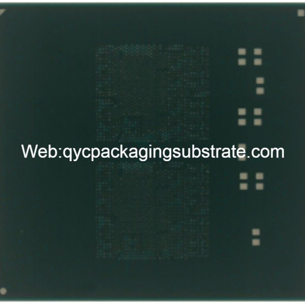
Embedded wafer-level-packages fan-out wlp chip embedded in substrate
Foundations of Wafer-Level Packaging (WLP)
Wafer-Level Packaging (WLP) represents an advanced packaging technology that integrates chip packaging directly onto the wafer itself. This signifies that, in the final stages of chip manufacturing, packaging and interconnections occur directly on the wafer, as opposed to individual chips being packaged independently and subsequently connected to a substrate. The fundamental principle underlying WLP involves applying packaging materials onto the chip’s surface, followed by employing microprocessing and packaging technologies to establish connections between the chip and the substrate.
The design of WLP typically includes encapsulation materials such as adhesives and metal wire connections to ensure chip protection and stability. These materials require precise placement and micro-processing to achieve reliable connections and protection. The design of WLP also depends on the chip’s purpose and performance requirements, so different application areas may require different types of WLP.
WLP is widely used in packaging substrates because of its multiple advantages. First, WLP can significantly reduce the size of the package, making it more compact, which is crucial for the design of small electronic devices. Secondly, WLP can provide lower inductance and better electrical signal transmission, thereby improving the performance of the chip. In addition, WLP can also reduce the cost of packaging because it reduces additional connection and assembly steps.
Wafer-Level Packaging (WLP) is a pivotal technology in the contemporary electronics industry, finding widespread application in a variety of products, including smartphones, tablets, sensors, and MEMS (micro-electromechanical systems) devices, among others. Its compact design and high-performance attributes make WLP the preferred packaging technology for cutting-edge electronic devices.
In essence, the fundamental principle of WLP revolves around achieving reliable connections and protective encapsulation through the application of packaging materials on the chip’s surface, followed by micro-processing and packaging techniques. This technology has a significant impact on packaging substrates, offering a compact and high-performance solution that holds great importance for the advancement of the electronics industry. It merits careful attention and in-depth exploration.
Varieties of Fan-Out WLP
Within the domain of Wafer-Level Packaging (WLP) technology, various types of WLP exist, each possessing unique characteristics and applications. These include Basic WLP, Embedded WLP, and Fan-Out WLP, each playing distinct roles in package substrate design.
Basic WLP: The Traditional Form of WLP
Basic WLP typically embraces a thin and miniaturized design, characterized by low cost, low power consumption, and high performance. This type of WLP is commonly deployed in small electronic devices like smartphones, tablets, and wearable gadgets.
Embedded WLP: Redefining Packaging Substrates
Embedded WLP is a relatively novel form of WLP distinguished by its core feature of embedding the WLP chip within the package substrate, rather than connecting it to the substrate’s surface. This approach offers the advantage of reducing the overall package size, enhancing circuit reliability and performance. Embedded WLP also facilitates greater chip density, as the chips can be positioned closer to the substrate’s surface. This type of WLP is frequently harnessed in high-density packaging, embedded systems, and miniature sensors.
Fan outlet type WLP: Detailed description of the features and advantages of fan outlet type WLP
The fan outlet type WLP is a variant of WLP whose design is inspired by the working principle of a fan. In this type of WLP, the chip is packaged in a packaging substrate with tiny air outlets. These air outlets are used for heat dissipation and air circulation to keep the chip running at low temperatures.
These different types of WLP play different but critical roles in packaging substrate technology, helping to meet the needs of various electronic devices. By selecting the appropriate WLP type, you can find the ideal balance between size, performance and reliability to meet the needs of different application areas.
Application of embedded WLP chips in packaging substrates
Embedded Wafer-Level Package (WLP) chips have a wide range of applications. They not only provide innovative solutions in the electronic field, but also play a key role in many fields. The following are some of the diverse applications of embedded WLP chips and their key role in the electronics field:
Smartphones and mobile devices:In modern smartphones and mobile devices, space and performance go hand in hand. Embedded WLP chips enable more compact designs while delivering superior performance, which is an important advantage for both mobile phone manufacturers and users. This packaging technology is widely used in processors, radio frequency modules and sensors to ensure that devices provide excellent performance in a small form factor.
Internet of Things (IoT) devices:IoT is a typical application of connectivity and miniaturization, so the small size and high performance of embedded WLP chips make them ideal for IoT devices. From smart home devices to medical devices, embedded WLP chips play a key role in enabling wearable technology and remote monitoring.
vehicle electronics:Modern cars are packed with electronic systems, including driver assistance technology, entertainment systems and vehicle communications. Embedded WLP chips can provide highly reliable solutions for harsh environmental conditions and facilitate smaller designs, improving vehicle performance and safety.
Telecommunication:Embedded WLP chips have a wide range of applications in wireless communication equipment, including base stations and network routers. Its small form factor and excellent RF performance make it ideal for high-speed data transmission and connectivity.
Medical equipment:In medical devices, accuracy and reliability are critical. Embedded WLP chips enable miniaturized medical devices while providing excellent performance and stability. This is critical for patient monitoring, medical imaging and medical diagnostic equipment.
The effective utilization of embedded Wafer-Level Package (WLP) chips in these applications underscores their indispensable contribution to the electronics sector. These chips not only enhance product performance but also catalyze innovation, offering users more sophisticated solutions. The ongoing progress in these chips will persist in spearheading advancements within the electronics industry, enabling the creation of smaller, higher-performing designs across a broader spectrum of applications.
Embedded wafer-level-packages fan-out wlp chip embedded in substrate
Advantages and applicability of different WLP types
Choosing the right wafer-level packaging (WLP) type is a crucial decision that hinges on a comprehensive understanding of their respective performance and attributes. In the following comparison, we aim to elucidate the performance and distinguishing features of various WLP types, offering readers valuable insights to facilitate the selection of the most suitable WLP type for their specific needs.
Compare the performance and features of different WLP types
Basic WLP:Basic WLP is a traditional packaging technology typically used in small and lightweight applications.
Embedded WLP:Embedded WLP provides higher density and performance by embedding the chip into the packaging substrate. It can be suitable for medium to highly complex applications such as mobile devices and some consumer electronics.
Fan outlet type WLP:The fan outlet type WLP adopts an advanced heat dissipation design, allowing it to perform well in high-performance and high-temperature environments. This makes it suitable for areas such as high-performance computing and communications equipment.
When choosing the appropriate WLP type, you need to consider the following factors:
Application requirements:First, figure out what your application needs are. If a small, lightweight package is required, basic WLP may be sufficient. And if you need higher performance and density, a recessed or fan-exhaust WLP may be more suitable.
Cost considerations:Consider budget and cost constraints. Basic WLP typically costs less, but for high-performance needs, investing in more advanced WLP technology may be necessary.
Performance requirements:Assess your application performance needs. If you need higher processing power, cooling performance or connectivity performance, it is crucial to choose the WLP type.
Environmental conditions:Understand the environmental conditions under which your application will run. If extreme conditions such as high temperatures or high humidity exist, a fan-exhaust WLP may be a better choice.
future development:Consider future technology trends. Choose a WLP type that is flexible and can adapt to future application changes.
In short, understanding the performance and characteristics of different WLP types, as well as considering factors such as application requirements, cost, performance, environment and future development, will help readers better choose the WLP type that suits their needs.
Future trends
The development prospects of Embedded Wafer-Level Package (WLP) technology in the electronics industry are exciting. The following will discuss future development trends and key points, emphasizing the indispensability of continuous innovation.
Predict the future development direction of WLP technology
Smaller, more powerful package:In the future, WLP technology will develop in the direction of smaller, thinner, and more powerful packages. This means higher packaging density, more functions integrated on one chip, and reduced package size. This trend will promote the further development of embedded WLP technology and adapt to a wider range of applications.
More complex materials and structures:As technology develops, new materials and packaging structures will continue to emerge. These materials will provide better electrical performance, thermal performance and mechanical strength to meet the needs of more applications. Embedded WLP will be an ideal choice for adopting these innovative technologies.
Advanced heat dissipation and packaging technology:As the performance requirements of electronic devices continue to increase, heat dissipation and packaging technology will become the focus of future attention. Future embedded WLP technology will pay more attention to efficient heat dissipation solutions to ensure that the chip maintains stability under high loads.
Continuous innovation is crucial to the development of WLP technology. Innovation is driving the emergence of new materials, manufacturing processes and design methods that increase the performance and versatility of WLP technology. Manufacturers and R&D teams are encouraged to continue to explore new solutions and continuously improve WLP technology to adapt to changing market needs.
In addition, sustainable practices are also an important direction for the future. Reducing waste, energy consumption and environmental impact will become a key focus of WLP technology development. Through innovative sustainable approaches, we can drive progress in electronics while protecting our environment.
In summary, the future of embedded WLP technology is promising, and through continued innovation and a focus on sustainability, we can advance the electronics industry and meet growing demands while protecting our planet. The prospects for this field are exciting, and we look forward to seeing how future WLP technologies will shape our world.