 Professional Flip-Chip Packaging Substrate Supplier

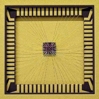
What is Wire Bonding BGA substrate?
Wire Bonding BGA substrates Manufacturer. High speed and high frequency material BGA packaging substrate Manufacturer. Advanced Msap and Sap production process. we offer Wire Bonding BGA substrates from 2 layer to 22 layers.
Wire Bonding BGA substrate (Ball Grid Array) is a special type of printed circuit board (PCB) that uses wire bonding technology for precise interconnections between semiconductor devices. Compared with traditional printed circuit boards, Wire Bonding BGA substrates have higher density, better thermal management performance and stronger mechanical stability, so they are widely used in high-performance electronic fields such as aerospace, automotive and communications. .
Wire Bonding BGA substrates usually have a ball grid array (Ball Grid Array) configuration, in which semiconductor devices are connected to the surface of the substrate through tiny solder balls. Wire Bonding technology achieves reliable electrical connections by bonding small metal wires between semiconductor devices and substrates. This dual connection method ensures the stability and reliability of the electronic system under various environmental conditions.
The uniqueness of this substrate design is that it adapts to the needs of high-density integrated circuits and miniaturization design, making it possible to implement complex circuit layouts in limited space. The manufacturing of Wire Bonding BGA substrates requires precision processes and advanced equipment to ensure the accuracy and reliability of tiny wire bonding and solder ball connections.
In general, Wire Bonding BGA substrate is a high-performance, high-density printed circuit board that uses advanced wire bonding technology to achieve reliable interconnection between semiconductor devices, providing a foundation for the design and manufacturing of modern electronic systems. Provided critical support and solutions.
Wire Bonding BGA substrates
How is the design of Wire Bonding BGA substrate carried out?
The design of Wire Bonding BGA substrates is a precise and meticulous process that determines the performance, reliability and serviceability of the final product. During the design phase, engineers need to consider many factors to ensure that the substrate can meet the needs of complex electronic systems.
First, the design team needs a detailed understanding of the project’s technical requirements and functional specifications. This may involve analysis of the circuit’s performance, power consumption, size, and layout. The key to this stage is to clarify the customer’s needs and expectations so that they can be accurately implemented in subsequent designs.
Next, the design engineer uses professional electronics design software, such as Altium Designer or Cadence Allegro, to begin creating the initial circuit board layout. In doing so, they need to consider signal integrity, power distribution, thermal requirements, and manufacturing feasibility. Through careful layout design, design teams can minimize signal interference and electromagnetic compatibility issues, ensuring substrate reliability and stability.
Once the preliminary layout is complete, the design engineer proceeds with the circuit board layer stackup design. This includes determining the substrate hierarchy, material selection, and how each layer functions and connects. Different layers may include power supply layers, ground layers, signal layers, and special functional layers such as electric heating layers or impedance matching layers.
After the board layout and layer stackup design is determined, the design team proceeds with routing and connection planning. They will design and optimize the paths of signal and power lines according to the requirements of the circuit layout to minimize signal delays and power losses. This step typically requires the use of electromagnetic simulation tools for signal integrity and electromagnetic compatibility analysis to ensure that the design meets expected performance specifications.
Finally, the design engineer conducts a thorough review and verification of the design. They use prototyping techniques to create samples for functional testing and performance evaluation. If necessary, they will modify and optimize the design until it meets the customer’s requirements and standards.
To sum up, the design process of Wire Bonding BGA substrate involves several key steps, including circuit layout, layer stacking, routing planning and verification. Through careful design and continuous optimization, the design team can achieve accurate realization of customer needs, thereby laying a solid foundation for the successful implementation of electronic systems.
What is the manufacturing process of Wire Bonding BGA substrate?
The manufacturing process of Wire Bonding BGA substrates is a complex process that is carefully designed and executed with precision. The main steps of this process are detailed below:
Material Selection: First, the manufacturer carefully selects the substrate material suitable for the specific application. Common materials include FR-4 glass fiber composite materials, polyimide films, and ceramic substrates. Material selection depends on required electrical performance, thermal management capabilities and mechanical stability.
Design and Layout: After deciding on the materials, the design team began working on the layout of the substrate. They consider factors such as signal integrity, power distribution, heat dissipation and more, utilizing advanced CAD software for design and simulation to ensure optimal performance and manufacturability.
Layer stacking: Layering of substrates is an important step at the beginning of the manufacturing process. This involves stacking thin layers of various materials together to form a complete substrate structure.
Circuit pattern production: Next, photolithography technology is used to form a circuit pattern on the surface of the substrate. This involves applying photoresist, exposing the photoresist, and chemically etching or etching areas not protected by the photoresist to create the desired circuit pattern on the substrate.
How much does it cost to manufacture a Wire Bonding BGA substrate?
When talking about the manufacturing cost of Wire Bonding BGA substrates, multiple factors need to be considered, such as material cost, design complexity, manufacturing process, production scale and market demand. Below we take a closer look at how these factors impact costs.
First of all, material cost is one of the important factors that determines the manufacturing cost of Wire Bonding BGA substrate. Different types of substrate materials have different prices, such as common FR-4, polyimide and ceramic substrates, and their costs vary greatly. Additionally, special material handling and surface treatments may add additional costs.
Secondly, design complexity has a direct impact on cost. Designing complex substrates may require more layers, finer circuit layouts and more complex structures, all of which increase manufacturing costs. In contrast, a simple design may reduce costs but may compromise on meeting functional and performance needs.
The manufacturing process is also a significant component of cost. Some advanced manufacturing processes, such as laser drilling, microvia technology and precision line pattern production, may increase manufacturing costs. The use of traditional processes and automated production lines can help reduce costs.
In addition, production scale is also one of the factors affecting costs. Generally speaking, large-scale production can achieve economies of scale and reduce the production cost of each substrate. Therefore, mass production is usually more economical than small batch production.
Finally, market demand and competitive conditions also have an impact on costs. If market demand is strong, manufacturers can reduce costs by increasing production capacity and efficiency to meet market demand. On the other hand, intense competition may lead to price competition that drives down manufacturing costs.
In general, the manufacturing cost of Wire Bonding BGA substrate depends on the combined influence of multiple factors. In order to control costs and achieve the best price/performance ratio, manufacturers need to comprehensively consider the above factors and take appropriate measures to optimize design, technology and production processes.
What material is the Wire Bonding BGA substrate made of?
After the circuit pattern is formed, the substrate undergoes a metallization process, often including a copper plating process, to increase conductivity and strengthen circuit connections.
Final processing: After the metallization treatment is completed, the final processing steps are performed on the substrate, including surface coating with a protective layer and final surface treatment to ensure the stability and reliability of the substrate.
Wire Bonding: For Wire Bonding BGA substrate, wire bonding is a critical step. In this process, tiny metal wires are ultrasonically welded to the surface of the semiconductor device and substrate to achieve electrical connection. This requires highly sophisticated equipment and technology to ensure welding accuracy and reliability.
Through the above steps, the Wire Bonding BGA substrate is manufactured, providing a reliable foundation for various high-performance electronic systems. This manufacturing process requires manufacturers to have advanced technology and extensive experience to ensure that the final product meets high standards of quality and performance requirements.
Who makes Wire Bonding BGA substrates?
In the field of Wire Bonding BGA substrate manufacturing, supplier selection is crucial. Ensuring that partners have technical prowess, production capabilities and reliability is critical to product quality and project success. Let’s explore our company’s role in Wire Bonding BGA substrate manufacturing.
As one of the suppliers of Wire Bonding BGA substrates, our company is committed to providing high quality, reliability and innovative solutions to meet the growing needs of our customers. We have advanced manufacturing facilities and technical capabilities to provide customers with a full range of services and support.
First, our team consists of experienced engineers and technical experts who have deep expertise in PCB design and manufacturing. From initial conceptual design to final production and manufacturing, we can provide full technical support and guidance to ensure that customer needs are fully met.
Secondly, we focus on quality management and optimization of production processes. We adopt an advanced quality control system to ensure that every process complies with strict quality standards and industry specifications. From raw material procurement to production and manufacturing, we strictly control every detail to ensure the quality of the final product is stable and reliable.
In addition, we actively invest in technological innovation and equipment updates. We continue to introduce the latest manufacturing technology and equipment to improve production efficiency and product quality to meet our customers’ growing needs and challenges.
Most importantly, we focus on close cooperation and communication with our customers. We know that our customers’ needs and expectations are the source of motivation for us to move forward, so we always maintain open communication channels, listen to customer feedback and suggestions, and constantly optimize and improve our products and services.
To sum up, as a supplier of Wire Bonding BGA substrates, our company is committed to providing high-quality, reliable and innovative solutions, and working with customers to create a better future. Look forward to working with you!
What are the five characteristics of great customer service?
Excellent customer service is one of the keys to business success, and in the Wire Bonding BGA substrate manufacturing industry, providing excellent customer service is especially important. The following is a detailed introduction to the five characteristics of excellent customer service:
Timely response and communication: During the Wire Bonding BGA substrate manufacturing process, customers may have various questions, needs or opinions. The number one characteristic of great customer service is prompt response and communication. Customers should be able to get a quick response to any questions they have. By establishing effective communication channels, including phone, email and online chat, ensure that customers can contact the company at any time and receive timely support and assistance.
Professional technical support: In the Wire Bonding BGA substrate manufacturing industry, customers may require in-depth technical support to solve complex design or manufacturing problems. The second characteristic of excellent customer service is providing professional technical support. Companies should have a team of experienced technical experts who can provide customers with accurate and comprehensive solutions and help them overcome the challenges they encounter.
Flexibility and adaptability: Customer needs are often changing, so companies need to be flexible and adaptable to meet the individual requirements of different customers. The third characteristic of quality customer service is the ability to flexibly adjust production plans, customize product specifications, and promptly respond to customer change requests. By building close relationships with customers, companies can better understand their needs and make timely adjustments to meet their expectations.
Quality Assurance: In the Wire Bonding BGA substrate manufacturing industry, quality is crucial. The fourth characteristic of excellent customer service is providing strict quality assurance. Companies should implement strict quality control measures to ensure that every substrate produced meets customer specifications and industry standards. At the same time, enterprises should also actively participate in continuous improvement activities to continuously improve product quality and production efficiency.
After-sales support: Quality customer service includes not only providing support during the sales process, but also providing ongoing support and assistance to customers during the after-sales phase. Companies should provide customers with comprehensive after-sales services, including product installation guidance, troubleshooting and maintenance suggestions. By responding to customer feedback and complaints in a timely manner and proactively resolving issues, companies can win customers’ trust and loyalty and establish long-term and solid cooperative relationships.
In summary, excellent customer service is the key to a company’s success in the Wire Bonding BGA substrate manufacturing industry. Through timely response and communication, providing professional technical support, flexible adjustment of production plans, strict quality assurance and complete after-sales support, enterprises can win the trust and satisfaction of customers and achieve common development.
FAQS
How is Wire Bonding BGA substrate distinguished from other types of PCBs?
Wire Bonding BGA substrate adopts ball grid array configuration and uses wire bonding technology to connect semiconductor devices. It is different from traditional PCB in structure and connection method. This design enables Wire Bonding BGA substrates to have superior electrical performance and reliability in high-performance electronic devices.
How long does it take to manufacture a Wire Bonding BGA substrate?
The time to manufacture a Wire Bonding BGA substrate depends on several factors, including design complexity, manufacturing process, production scale, and supply chain efficiency. Generally speaking, it can take anywhere from a few weeks to a few months from design to final delivery.
What factors mainly determine the cost of Wire Bonding BGA substrate?
The cost of Wire Bonding BGA substrates is affected by many factors, including substrate material, design complexity, manufacturing process, production quantity and technical specifications. High-performance substrates and customization requirements often result in higher costs, but large-scale production and efficient manufacturing processes can help reduce overall costs.
What are the common problems you may encounter when manufacturing Wire Bonding BGA substrates?
During the manufacturing process of Wire Bonding BGA substrates, you may encounter challenges such as material selection, process control, bonding quality, inter-layer connection, etc. Effective quality control and process optimization are the keys to solving these problems.
What applications are Wire Bonding BGA substrates suitable for?
Wire Bonding BGA substrates are widely used in various high-performance electronic systems, including microprocessors, memory modules, wireless communication equipment, medical equipment, military aerospace and other fields. Its superior electrical performance and reliability make it the first choice for many critical applications.