 Professional Flip-Chip Packaging Substrate Supplier

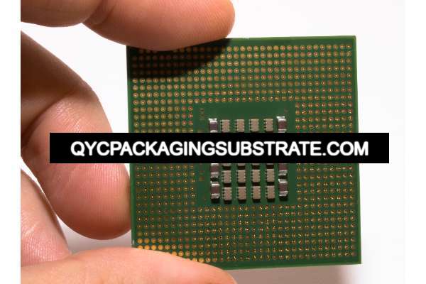
What is WLP Package Substrate?
WLP Package Substrate Manufacturer. We use advanced Msap and Sap technology, High multilayer interconnection substrates from 2 to 20 layers,High quality and fast shipping time. Our company also offer WLP Package Service.
WLP Package Substrate (Wafer-Level Package Substrate) is a special substrate used in the wafer-level packaging (Wafer-Level Packaging, WLP) process. It is a key component in electronic device packaging, responsible for providing the basis for supporting and connecting semiconductor chips, thereby enabling the integration of high-density components.
In the wafer-level packaging process, the chip and the substrate are packaged on the same wafer. Compared with traditional packaging methods, WLP Package Substrate has lower manufacturing costs and a more efficient packaging process. It allows multiple chips to be packaged on the same wafer at the same time, reducing subsequent assembly processes and improving production efficiency.
The main role of WLP Package Substrate is to provide a reliable platform for mounting and connecting chips, while also protecting the chip from the external environment. It provides an electrical connection to the chip and also has good heat dissipation properties, helping to maintain a stable operating temperature of the chip. Therefore, WLP Package Substrate plays an important role in realizing high-performance, high-reliability electronic device packaging.
WLP Package Substrate
As an innovative electronic packaging technology, WLP Package Substrate (wafer level packaging substrate) has many types, each type is targeted at specific application scenarios and requirements. The following are several common WLP Package Substrate types and their characteristics and applicability:
FO-WLP is an advanced packaging technology that enables high-density packaging by connecting an expanded array of electrodes around the chip to another substrate at the wafer level. It is suitable for applications that require a high degree of integration and miniaturization, such as smartphones, tablets, and wearable devices.
FI-WLP is another common WLP Package Substrate type, which is characterized by directly connecting the electrodes of the chip to the substrate to achieve compact packaging. It is suitable for applications requiring lower cost and medium-density packaging, such as consumer electronics and automotive electronics.
CSP is a compact package that is comparable in size to the chip, minimizing the overall size of the package. It is suitable for applications requiring high integration and high performance, such as mobile communication equipment, medical equipment and industrial control.
eWLB is an advanced packaging technology that directly packages chips on a substrate, with high density and reliability. It is suitable for applications requiring high performance and reliability, such as aerospace, defense and medical equipment.
These WLP Package Substrate types have their own advantages and characteristics in terms of size, cost, integration and performance. Design engineers can choose the most appropriate type according to specific application requirements to achieve the best packaging effect.
What are the advantages of using WLP Package Substrate?
As an advanced packaging technology, WLP Package Substrate brings a series of unique advantages compared to traditional PCB, ranging from performance to reliability to miniaturization, and has been significantly improved.
First, WLP Package Substrate provides excellent thermal management capabilities. Compared with traditional PCB, the heat conduction path of WLP Package Substrate is more direct, which can more effectively transfer the heat generated by the chip, reduce the accumulation of hot spots, and improve the overall heat dissipation effect. This enables WLP Package Substrate to maintain a stable operating temperature in high power density applications, thereby enhancing the reliability and lifespan of electronic devices.
Second, WLP Package Substrate enables a higher degree of integration and miniaturization. By packaging the chip directly on the surface of the substrate, WLP Package Substrate can significantly reduce the connection length and spacing between components, allowing for a more compact layout. This not only reduces the size and weight of the circuit board, but also improves the integration of the system, which is conducive to the design of more compact and lightweight electronic products, meeting the continuous demand for miniaturized equipment in today’s market.
In addition, WLP Package Substrate also has excellent electrical performance. Because it is directly packaged on the surface of the substrate, the electrical signal transmission path is shorter, the impedance matching is more accurate, and the signal loss in the circuit is smaller. This makes WLP Package Substrate excellent in high-frequency and high-speed signal transmission applications, helping to improve system performance and reliability.
In addition, WLP Package Substrate has the advantage of lower manufacturing costs. Compared to traditional PCB manufacturing processes, WLP Package Substrate’s manufacturing process is more streamlined and consumes less material and energy. At the same time, since multiple chips can be packaged on the same substrate at the same time, assembly steps and material usage are reduced, and the overall manufacturing cost is reduced. This makes the WLP Package Substrate more competitive in mass production, helping to reduce the overall cost of the product.
In summary, WLP Package Substrate, as an advanced packaging technology, has many advantages, including excellent thermal management capabilities, higher integration and miniaturization, excellent electrical performance, and lower manufacturing costs. These advantages make WLP Package Substrate an important choice in today’s electronic product design, bringing more advanced, reliable and efficient solutions to various industries.
Why choose WLP Package Substrate?
WLP Package Substrate, as an innovative electronic packaging solution, has obvious advantages compared with traditional PCB. Here are a few key benefits of choosing WLP Package Substrate:
WLP Package Substrate allows the integration of more components in a smaller package space. Compared with traditional PCB, it can achieve higher-density component layout, making electronic devices more compact in size and suitable for application scenarios with strict size requirements.
The design of WLP Package Substrate takes the importance of thermal management into consideration, effectively improving the heat dissipation efficiency of the chip through shorter interconnect length and higher heat dissipation performance. This means that in high power density applications such as servers, embedded systems, etc., WLP Package Substrate can maintain component stability and reliability.
Because the connections between components are shorter and more direct in WLP Package Substrate, there is lower resistance and signal delay. This makes WLP Package Substrate perform better in high-speed data transmission and signal integrity, making it suitable for applications with strict signal transmission requirements.
The design of WLP Package Substrate reduces inductance and capacitance between components, reducing the possibility of signal interference. In addition, since the number of welds and connections is reduced, potential points of failure are also reduced, thereby increasing the reliability of the entire system.
Compared with traditional PCBs, the manufacturing process of WLP Package Substrate is more streamlined and efficient. The use of wafer-level packaging technology can achieve mass production, greatly shortening the production cycle, and also reducing manufacturing costs due to the optimization of materials and processes.
To sum up, WLP Package Substrate has many advantages over traditional PCB, including higher integration, excellent thermal management performance, lower resistance and delay, higher reliability and anti-interference, and faster production cycle and lower costs. Therefore, choosing WLP Package Substrate is a wise choice when facing electronic applications that require higher size, performance and reliability.
What is the manufacturing process of WLP Package Substrate?
The manufacturing process of WLP Package Substrate is a complex and precise process designed to achieve high-density, high-performance packaging solutions. Below we’ll take a closer look at its key steps:
The first step in the manufacturing process is to thoroughly clean and prepare the silicon wafer. This includes removing surface impurities and dirt to ensure the accuracy and reliability of subsequent processing steps.
Next, a redistribution layer (RDL) is formed on the wafer surface. RDL is a thin film used to redistribute the pins connected to the chip to conform to the desired layout and arrangement.
After the RDL is formed, the chip is precisely placed on the wafer and bonding technology is used to hold it in place. This step requires a high degree of precision and stability to ensure that the chip is properly connected to the redistribution layer.
After chip placement and bonding is complete, package fillers are injected into the voids of the wafer to fill any gaps and improve package stability and reliability. Encapsulating materials are then used to enclose and protect the chip and connection points.
The final step in the manufacturing process is testing and verification of the packaged WLP Package Substrate. This includes a thorough evaluation of connectivity, electrical performance, and physical reliability to ensure the final product meets specifications and quality standards.
Overall, the manufacturing process of WLP Package Substrate is a delicate and multi-step process that requires a high degree of process control and technical strength. By gradually completing key steps such as cleaning, redistribution layer formation, wafer placement and bonding, package filling and packaging, and testing and inspection, a high-quality, reliable WLP Package Substrate can be produced to meet the needs of different application fields.
What are the applications of WLP Package Substrate?
WLP Package Substrate is an advanced packaging technology that is widely used in multiple industries and fields to meet the needs of different applications. Here are some of the main applications of WLP Package Substrate:
WLP Package Substrate is widely used in consumer electronics products such as smartphones, tablets, and wearable devices. Its miniaturization, lightweight and high performance make it an ideal choice for manufacturing high-end electronic products. In addition, WLP Package Substrate can provide excellent thermal management to ensure stable operation of the equipment for a long time.
In automotive electronic systems, WLP Package Substrate plays a key role. It is used to manufacture automotive control units (ECUs), airbag systems, automotive entertainment systems and other components. Its high-density integration and reliability capabilities enable automotive electronic systems to meet increasingly complex functional and performance requirements.
Medical equipment has extremely high requirements for high performance and reliability, so WLP Package Substrate is widely used in medical equipment. For example, devices such as pacemakers, medical imaging equipment, and life support systems use WLP Package Substrate technology to ensure their stable performance and long-term reliability.
In industrial control systems, robotics and automation equipment, WLP Package Substrate delivers high performance and reliability. It can meet complex control and communication requirements, has high temperature resistance, corrosion resistance and other characteristics, and is suitable for various harsh industrial environments.
WLP Package Substrate is widely used in communication infrastructure, mobile communication equipment and satellite communication systems. Its high-frequency characteristics and excellent signal transmission performance enable communication equipment to achieve high-speed data transmission and stable communication connections.
To sum up, WLP Package Substrate plays an important role in multiple industries and applications, providing various electronic products with advantages in performance, reliability and miniaturization, and promoting the development and application of modern electronic technology.
Where can I find WLP Package Substrate?
You can find high-quality WLP Package Substrate in our company to provide reliable solutions for your projects. As a leading electronic packaging supplier, we are committed to providing various types of WLP Package Substrate to meet your different needs.
Ensure Supply Quality: Our WLP Package Substrate is manufactured by a team of experienced professionals using advanced manufacturing processes and strict quality control processes. We strictly follow international standards to ensure product quality and stability.
Customized services: We provide customized solutions and customize WLP Package Substrate according to your specific requirements and application scenarios. Whether it’s size, material or special requirements, we can tailor it for you to ensure the product exactly meets your needs.
Provide technical support: We have a professional technical team that can provide you with comprehensive technical support and consulting services. Whether it is choosing the right product model or technical difficulties in the manufacturing and application process, we can provide you with help and solutions.
Flexible delivery methods: We offer flexible delivery methods to provide you with products in a timely manner based on your needs and schedule. Whether it’s a small batch order or mass customization, we can meet your needs and ensure timely delivery.
High cost-effectiveness: We are committed to providing cost-effective products and services to save you costs and improve efficiency. Our products are reasonably priced and of reliable quality, bringing long-term value and competitive advantage to your project.
By choosing our company as your WLP Package Substrate supplier, you can be assured of high-quality products and excellent service. We will wholeheartedly provide you with the most satisfactory solutions and work with you to create a better future.
What is the quote for WLP Package Substrate?
WLP Package Substrate’s quotation is affected by many factors. First of all, the type of WLP Package Substrate is one of the important factors that determines the price. Different types of WLP Package Substrate, such as Fan-Out WLP (FO-WLP), Fan-In WLP (FI-WLP), Chip-Scale Package (CSP), etc., have different design complexity and cost structures, so the prices also vary. will vary.
Secondly, the size and thickness of WLP Package Substrate will also directly affect its price. Generally speaking, larger size and thicker Substrate will consume more materials and production costs, so the price may be higher. In addition, if customers have customized requirements, such as a specific number of layers, metal layers, or special protective layers, this will also increase the manufacturing cost and final quotation.
In addition, purchase volume is also an important factor affecting WLP Package Substrate quotation. Typically, large-volume purchases can enjoy lower unit prices because manufacturers can reduce production costs through economies of scale. On the contrary, small batches or customized orders may result in higher unit prices because production efficiency is low and manufacturers require more resources for adjustment and debugging.
In addition, market supply and demand will also affect the price of WLP Package Substrate. If there is high demand for a certain type of Substrate and insufficient supply, prices may rise. Conversely, if the market is well supplied but not in demand, prices may fall.
To sum up, the price of WLP Package Substrate is affected by many factors, including type, size, customization requirements, purchase volume, and market supply and demand conditions. Therefore, when selecting and purchasing WLP Package Substrate, customers should comprehensively consider these factors and fully communicate with suppliers to obtain the most suitable quotation.
FAQS
How does WLP Package Substrate improve thermal management?
WLP Package Substrate enhances thermal management by reducing the distance between the semiconductor chip and the heat sink. This shorter path for heat dissipation minimizes thermal resistance, allowing for efficient heat transfer and dissipation, thus improving overall thermal performance.
Are WLP Package Substrates compatible with standard assembly processes?
Yes, WLP Package Substrates are designed to be compatible with standard assembly processes commonly used in the electronics industry. Manufacturers often ensure that WLP packages adhere to industry standards, making them suitable for integration into existing assembly lines without significant modifications.
What are the environmental considerations associated with WLP Package Substrates?
WLP Package Substrates typically utilize materials that comply with environmental regulations such as RoHS (Restriction of Hazardous Substances). Manufacturers prioritize the use of lead-free and environmentally friendly materials in the fabrication process to minimize environmental impact. Additionally, the compact size and efficient design of WLP Substrates contribute to reduced material usage and waste.
Can WLP Package Substrates support high-frequency applications?
Yes, WLP Package Substrates are capable of supporting high-frequency applications, thanks to their advanced design and optimized signal routing. The shorter interconnect lengths and reduced parasitic effects inherent in WLP structures enable high-speed signal transmission with minimal signal degradation, making them suitable for demanding high-frequency applications such as RF (Radio Frequency) devices and wireless communication modules.
What is the longevity and reliability of WLP Package Substrates?
WLP Package Substrates are engineered to deliver exceptional longevity and reliability. Through rigorous testing and quality assurance measures during manufacturing, WLP Substrates undergo stringent reliability assessments to ensure compliance with industry standards. Additionally, the compact and robust nature of WLP structures minimizes the risk of mechanical failures and enhances overall product reliability, making them suitable for mission-critical applications where reliability is paramount.