 Professional Flip-Chip Packaging Substrate Supplier

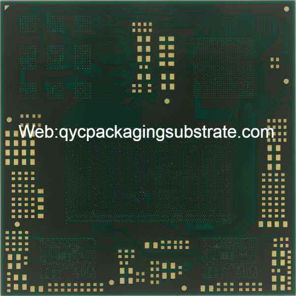
Professional BGA Substrate Manufacturer, Characteristic: ultra-small bump pitch, ultra-small trace and spacing. Mitsubishi BT base materials, ABF base materials, Rogers base materials. and other types materials.
In today’s rapidly developing field of electronic technology, Ball Grid Array (BGA) Substrate is an indispensable key circuit board component. Its unique design and functions are widely used in various modern electronic equipment. BGA Substrate using ball grid array layout not only provides reliable connections to the chip, but also plays an important role in electrical performance.
What makes BGA Substrate unique is its ball grid array layout, a design that has become a key connectivity element in modern electronic devices with its highly compact arrangement. By arranging the solder balls on the bottom of the circuit board, BGA Substrate effectively increases the connection density and provides space for more signal channels. This compact layout allows BGA Substrate to play an important role in miniaturized electronic devices, providing reliable electrical connections for modern mobile devices, communication equipment, and consumer electronics products.
BGA Substrate’s connection performance
BGA Substrate exhibits excellent performance in providing connections to chips. Due to its spherical connection point design, BGA Substrate can effectively reduce resistance and improve the stability of signal transmission. This design not only enhances electrical performance, but also better handles temperature changes and mechanical stress, thereby improving the overall reliability of the electronic device.
Application of BGA Substrate in electronic equipment
BGA Substrate is widely used in various types of electronic equipment, especially those with high performance and reliability requirements. From computer motherboards to communication equipment to consumer electronics, BGA Substrate plays a vital role. Its superior connectivity and design features make it an integral part of modern electronics manufacturing.
As electronic devices continue to pursue miniaturization, high performance and high reliability, BGA Substrate’s design and manufacturing technology are also constantly innovating and developing. Improved high-density interconnection manufacturing technology and advanced semi-additive manufacturing technology will further promote the performance and functionality of BGA Substrate and lay a solid foundation for the development of future electronic equipment.
What are the functions of BGA Substrate?
The Ball Grid Array Substrate (BGA Substrate) stands as a crucial element in PCB engineering, wielding a distinctive design and functionality that significantly influences the performance of contemporary electronic devices. A comprehensive comprehension of the functions of the BGA Substrate is essential for gaining a profound insight into its significance within the realm of electronic engineering.
BGA Substrate
First of all, one of the main functions of BGA Substrate is to provide electrical connections. Through its carefully designed ball grid array layout, BGA Substrate is able to achieve reliable electrical connections to the chip. This connection method not only provides a high degree of reliability, but also supports the transmission of complex circuits, providing a solid electrical foundation for the normal operation of electronic equipment.
Furthermore, the BGA Substrate assumes a crucial role in bolstering chip packaging, offering a robust framework that not only ensures the chip’s stability during installation and operation but also provides essential support for optimal chip performance. This support extends beyond mere mechanical protection, encompassing the isolation of the chip’s environment to mitigate external interference impacts.
In electronic devices, the BGA Substrate serves as a linchpin for reliable signal transmission. Its thoughtfully engineered design facilitates the conveyance of high-frequency signals while concurrently minimizing signal distortion during transmission. This feature is particularly critical in applications demanding high-speed data transmission, such as communication equipment and computer systems, where the BGA Substrate plays a pivotal role in fostering seamless communication between devices.
Lastly, the BGA Substrate emerges as a key player in power management. By efficiently regulating the flow of electrical current, it aids in minimizing the power consumption of electronic devices, thereby enhancing overall energy efficiency. This function is of particular significance in mobile devices and portable electronics, where battery life limitations often come into play.
In essence, the BGA Substrate has evolved into an integral component of contemporary electronic device design, delivering essential functions including electrical connections, support for chip packaging, reliable signal transmission, and efficient power consumption management. Its refined design and exemplary functions provide a sturdy foundation for innovation and development in the field of electronic engineering.
What are the different types of BGA Substrate?
In modern PCB engineering, BGA Substrate is one of the key components, and its different types involve multi-level classification of materials and designs. We’ll take a closer look at each of these types, as well as their advantages and characteristics in different application scenarios.
First, BGA Substrate’s material classification is an important aspect of its diversity. In this regard, we can divide BGA Substrate into different types, such as ceramic substrates, organic substrates, etc. Ceramic substrates are favored in high-performance applications due to their excellent thermal conductivity and mechanical strength, while organic substrates excel in a wide range of applications due to their lightweight, low cost, and adaptability.
Secondly, design-based classification also has a profound impact on the performance and applicable scenarios of BGA Substrate. For example, the design of multi-layer BGA Substrate can provide higher density and better signal integrity, making it widely used in high-demand electronic equipment. In contrast, single-layer designs are more suitable for cost-sensitive applications, such as some consumer electronics.
In different application scenarios, the advantages and characteristics of BGA Substrate are further highlighted. For high-performance computing and communication equipment, BGA Substrate using ceramic substrates can effectively manage heat and ensure reliable signal transmission. In thin and light portable devices, BGA Substrate using organic substrates can meet strict requirements on weight and thickness.
Taking these different types into consideration, manufacturers and engineers need to make informed choices based on their specific needs when designing circuit boards. At the same time, this also leads to continuous innovation and improvement of BGA Substrate’s manufacturing technology to meet the needs of increasingly complex and diverse electronic devices.
Overall, the different types of BGA Substrate provide the flexibility to achieve optimal performance in different application scenarios. With a deeper understanding of its materials and design, engineers can better select and optimize BGA Substrate, driving continued improvements in the performance and reliability of electronic devices.
What is the relationship between BGA Substrate and IC packaging? What are the classifications of chip packaging technology?
In the field of today’s electronic equipment manufacturing, Ball Grid Array (BGA) Substrate and Integrated Circuit (IC) packaging technologies are inseparable key components. We’ll delve into their close connections while understanding the diverse classification of chip packaging technologies to reveal their synergy in circuit board design.
The relationship between BGA Substrate and IC packaging
BGA Substrate is a specially designed circuit board commonly used for the packaging and connection of integrated circuits (ICs). Its ball grid array layout provides reliable electrical connections to the chips while allowing for higher pin density. The role of BGA Substrate in IC packaging is not only to provide physical support, but also to provide stable electrical connections for the chip, helping to ensure the reliability of signal transmission.
Classification of chip packaging technology
There are various chip packaging technologies, each with its own unique characteristics and applicable scenarios. The following are some common chip packaging technology classifications:
BGA packaging (Ball Grid Array): BGA packaging is a common IC packaging technology, characterized by spherical solder joints forming an array on the bottom of the chip. This is closely related to the design of BGA Substrate, providing a reliable connection.
QFN package (Quad Flat No-leads): The QFN package is a compact package with solder joints located on the four edges of the bottom of the chip. This packaging method performs well in terms of space utilization efficiency and heat dissipation performance.
TSOP package (Thin Small Outline Package): TSOP package is a thin small outline package, usually used for memory chips. Its low-profile design enables widespread use in height-constrained devices.
CSP package (Chip Scale Package): CSP package is a compact package with a size close to the actual size of the chip. It minimizes the impact of packaging on the overall size and improves circuit board integration.
BGA Substrate works synergistically with different types of IC packages to provide multi-layered advantages for circuit board design. By matching the appropriate packaging technology, designers can achieve higher pin density, better thermal performance, and more compact board layouts. This synergy allows electronic devices to be optimized in terms of size, performance and reliability.
In summary, the deep connection between BGA Substrate and IC packaging technology and their synergy in circuit board design form an indispensable part of modern electronic equipment manufacturing. Understanding these relationships will help in the design of more advanced, compact, and reliable electronic products.
What is the difference between BGA Substrate and PCB?
In the construction of modern electronic devices, Ball Grid Array (BGA) Substrate presents a series of striking differences compared with traditional printed circuit boards (PCBs). Through in-depth comparison, we can more fully understand their unique role in electronic devices.
First, let’s focus on the traditional PCB, a common basic building block in electronic devices. PCB usually serves as a support platform for electronic components, and electrical connections are achieved by printing conductive lines and inserting components. Motherboards, substrates, and substrate style circuit boards (SLP) are common forms of PCBs that play a key role in electronic devices. The motherboard is the core of the entire circuit board system, connecting various components to achieve the normal operation of the device. The substrate is the main component of the PCB, carrying the electronic components and providing electrical connections. The substrate style circuit board (SLP) uses a special design form to make the circuit board more compact and efficient.
However, BGA Substrate has distinguished itself among electronic devices with its unique design and layout. BGA Substrate uses a ball grid array layout to provide reliable connections and electrical performance for the chip. Compared with traditional PCB, BGA Substrate has significant advantages in space utilization and electrical performance. High-density interconnect substrate (HDI) is a form of BGA Substrate that enables higher performance and smaller size by increasing circuit density and reducing the distance between components.
The key difference is that BGA Substrate focuses more on providing more connections in a limited space and ensuring the reliability of electrical performance through the layout of the ball grid array. This design gives BGA Substrate significant advantages in electronic devices requiring miniaturization and high performance. Compared with traditional PCB forms, BGA Substrate is more suitable for modern electronic products that require compact design and high complexity.
Overall, there are significant differences in design, layout and performance between BGA Substrate and traditional PCB. Understanding these differences can help engineers better select circuit board construction methods for specific applications, ensuring device reliability and performance in demanding environments.
What are the main structures and production technologies of BGA Substrate?
In modern electronic engineering, Ball Grid Array (BGA) Substrate is a key technology, and its structure and production technology are directly related to the performance and reliability of electronic equipment. An in-depth understanding of the structure of BGA Substrate and its production technology, especially in terms of high-density interconnect (HDI) manufacturing technology and new manufacturing technology of semi-additive methods, is the key to understanding its functions and applications.
Structure of BGA Substrate
The structure of BGA Substrate is designed to provide maximum electrical connection performance in a small space. Its main structure includes substrate, metal layer, insulation layer and solder ball. The substrate usually uses high-performance materials, such as FR-4 or more advanced materials, to ensure the stability and reliability of the circuit board. The metal layer provides the electrical connection, while the insulating layer separates the metal layers and prevents electrical shorts. Solder balls play a vital role as a bridge connecting the chip and the circuit board.
Application of HDI Manufacturing Technology
High-density interconnect (HDI) manufacturing technology is an important innovation in the field of BGA Substrate. Through HDI technology, designers can achieve more electrical connections in a smaller area and increase the performance density of the circuit board. This involves the use of microscopic traces, smaller apertures and interlayer connections to bring electronic components closer together, thereby increasing signal transmission rates and reducing the overall size of the circuit board. This technology is critical to the design of modern compact electronic devices.
Innovation of semi-additive method
The semi-additive method represents a recent advancement in BGA substrate production, diverging from the traditional additive approach. In contrast, this innovative method minimizes waste generation and enhances production efficiency through a more precise processing procedure. Embracing this cutting-edge technology not only contributes to a more eco-friendly production environment but also proves instrumental in lowering production costs, offering electronic equipment manufacturers more competitive solutions.
A comprehensive grasp of the BGA substrate’s structure and production technology reveals a continuous push by manufacturers to advance technology while simultaneously optimizing structures and production processes. This dual focus ensures that modern electronic equipment meets the elevated standards of high performance and reliability. The ongoing trend of relentless innovation is poised to further propel the evolution of electronic engineering, ushering in a new era of advanced and dependable electronic products that seamlessly integrate into our daily lives.
BGA Substrate FAQs
When exploring the world of BGA Substrate, it naturally leads to a series of frequently asked questions about this critical component. The following are some common questions and their detailed answers to help readers better understand and apply the importance of BGA Substrate in PCB engineering.
What is the difference between BGA Substrate and traditional PCB?
Compared with the traditional Printed Circuit Board (PCB), BGA Substrate has significant differences in structure and function. Traditional PCBs are mainly used for connection and support of electronic devices, while BGA Substrate not only provides electrical connections, but also supports chip packaging, achieving more efficient signal transmission through ball grid array layout.
What is special about BGA Substrate in PCB design?
BGA Substrate has unique specialties in PCB design, enabling smaller and lightweight electronic devices through its compact design and high integration capabilities. This makes BGA Substrate ideal for modern high-performance devices.
What are the manufacturing technologies of BGA Substrate?
BGA Substrate’s manufacturing technology involves multiple levels, including improved high-density interconnect (HDI) manufacturing technology and new semi-additive manufacturing technology. The application of these technologies enables BGA Substrate to better meet the space utilization and performance requirements of advanced electronic devices.
What are the application fields of BGA Substrate?
BGA Substrate is widely used in many fields, including communications, computers, medical equipment, etc. Its excellent performance in high-performance equipment makes it the first choice in a variety of applications.
How to ensure the reliability of BGA Substrate?
To ensure the reliability of BGA Substrate, strict quality control and testing standards are adopted during the manufacturing process. This includes comprehensive testing of key aspects such as electrical connections and thermal management to ensure that BGA Substrate can operate stably under various environmental conditions.
What is the future development trend of BGA Substrate?
With the continuous advancement of electronic technology, the future development trend of BGA Substrate will mainly focus on improving integration, reducing energy consumption, and adapting to more complex application scenarios. This will provide a broader space for innovation and performance improvement of electronic devices.