 Professional Flip-Chip Packaging Substrate Supplier

Micro via PCB manufacturing. We offer HDI PCB with smallest via size 50um. the Minimum traces are 9um. the Minimum spacing are 9um. High-speed materials with high TG are most suitable for the production of such small-pitch PCBs.
In the field of modern electronics, Micro Via PCB (printed circuit board) manufacturing technology has attracted much attention. Micro Via PCB not only enables higher density wiring, but also provides more powerful performance for small devices. This article will delve into the key steps, materials, and market trends of Micro Via PCB manufacturing, as well as how to ensure customer service quality. Through these contents, readers will better understand the development and application prospects of Micro Via PCB technology.
What is Micro Via PCB?
Micro Via PCB, or microvia printed circuit board, is an advanced technology that uses tiny apertures in printed circuit board manufacturing. Compared with traditional printed circuit boards, Micro Via PCB has smaller apertures and higher circuit density, making it widely used in small electronic devices. The breakthrough of this technology is its ability to achieve higher wiring density, thereby achieving more functions and performance in a limited space.
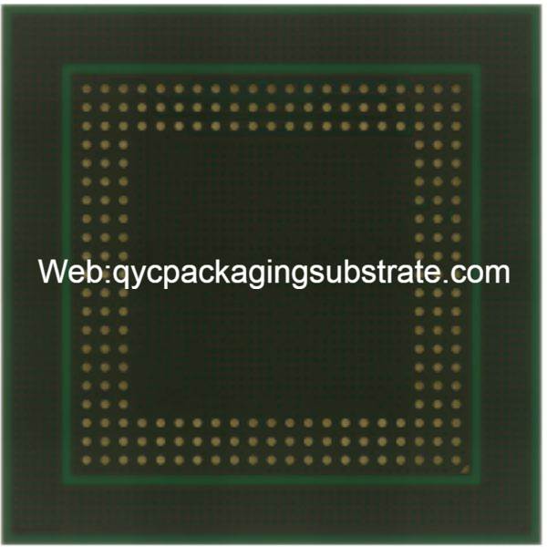
Micro via PCB manufacturing
The key to Micro Via PCB’s high-density wiring lies in its tiny aperture and precise manufacturing process. In traditional printed circuit board manufacturing, the hole diameter is larger, resulting in a larger spacing between lines, which limits the increase in circuit density. Micro Via PCB uses microvia technology to form tiny apertures on the PCB board, allowing circuits to be arranged more densely. The manufacturing of such tiny apertures requires high-precision processing equipment, such as laser drilling or mechanical drilling technology, to ensure the accuracy and consistency of the apertures. Through this precision manufacturing process, Micro Via PCB enables higher density wiring, resulting in more powerful performance in small devices.
The design of Micro Via PCB also needs to take into account the challenges of signal integrity and electrical performance caused by microvia wiring. Therefore, design engineers need to use professional PCB design software and accurately consider layout and routing to ensure the stability and reliability of signal transmission.
In general, Micro Via PCB achieves high-density wiring through microvia technology, providing more possibilities for the design and manufacturing of small electronic devices. It plays an important role in improving the performance and functionality of electronic products and is one of the important technologies in the field of modern electronic engineering.
What are the key points in designing Micro Via PCB?
Designing a Micro Via PCB is a complex and delicate process that requires the consideration of multiple factors to ensure the performance and reliability of the final product. Here are the key factors to consider when designing a Micro Via PCB:
Wiring density: The design of Micro Via PCB needs to take into account the requirements of high-density wiring to achieve more connections and functions in a smaller space. Optimizing routing density can improve board performance and efficiency.
Microvia location and size: Microvia location and size are critical to Micro Via PCB performance. Designers need to accurately determine the location of microvias and ensure that they are sized to meet the routing needs of the circuit board, while keeping the distance between microvias small enough to increase routing density.
Signal integrity: In Micro Via PCB design, signal integrity must be considered, including signal transmission stability, anti-interference ability and noise level. Signal distortion and crosstalk can be minimized by using proper routing techniques and signal routing.
Thermal management: High-density wiring in Micro Via PCBs can lead to localized heat concentrations, so designers need to consider effective thermal management solutions to ensure that the board can maintain a stable temperature during operation. This includes selecting appropriate thermal materials and laying out the cooling components.
Material Selection: Selecting the appropriate substrate material is critical to Micro Via PCB performance and stability. Designers need to consider the dielectric constant, thermal expansion coefficient, mechanical strength and other properties of the substrate material and select the appropriate material based on the specific application.
Cost-Effectiveness: When designing Micro Via PCBs, there must be a balance between performance and cost. Strategies such as optimizing routing and reducing the number of layers and microvias can reduce manufacturing costs without affecting board performance and quality.
To sum up, designing Micro Via PCB requires comprehensive consideration of multiple factors such as wiring density, microvia design, signal integrity, thermal management, material selection, and cost-effectiveness. Through careful design and optimization, high-performance, high-reliability Micro Via PCB can be realized to meet the needs of various applications.
What is the manufacturing process of Micro Via PCB?
When manufacturing Micro Via PCBs, a series of precise and complex steps are required to ensure the quality and performance of the final product. Following are the main steps in manufacturing Micro Via PCB:
Before entering the manufacturing phase, the PCB design first needs to be verified. This includes ensuring that design documents comply with specifications and are free of potential errors or issues.
The first step in manufacturing Micro Via PCB is to prepare the substrate material. This may involve cutting the substrate to the appropriate size and ensuring the surface is clean for subsequent processing.
PCB design files are often converted into graphical layouts to accurately locate microvia locations and routing paths during the manufacturing process.
The design pattern is transferred to the substrate surface using photolithography technology. This usually involves coating a photosensitive resin on the surface of a substrate and then forming a pattern through an exposure and development process.
Next is the step of drilling holes in the PCB. Use laser drilling or mechanical drilling techniques to create tiny apertures in the substrate as per the design requirements.
After drilling is completed, the hole walls need to be metallized, usually using electroless copper plating or other metallization methods to ensure good electrical conductivity and reliable connectivity.
Next is a chemical etching process that removes unwanted metal and creates the desired lines and apertures. This step requires precise control to avoid over-corrosion or under-etching.
After chemical etching is completed, different PCB layers are laminated and stacked according to the design requirements to form a complete Micro Via PCB structure.
Finally, photolithography and pad processing are used to form the final circuit pattern and connection points. This step ensures Micro Via PCB connectivity and reliability.
The above steps show the main process of manufacturing Micro Via PCB. Each step requires sophisticated equipment and technology to ensure the quality of the final product meets requirements.
How much does it cost to manufacture a Micro Via PCB?
The cost of manufacturing Micro Via PCB depends on several key factors that affect the expenses throughout the production process. Here are some of the main factors:
Design complexity: The design complexity of Micro Via PCB directly affects the manufacturing cost. If the design requires features such as high-density wiring, multi-layer boards, complex signal and power separation, etc., then the manufacturing cost will usually be relatively high. This is because design complexity increases process and material costs during manufacturing.
Pore size: The diameter of the micropores in Micro Via PCB has a great impact on manufacturing costs. Generally speaking, smaller apertures result in higher manufacturing costs because manufacturing tiny apertures requires more sophisticated processing equipment and higher production costs. Therefore, the manufacturing cost of Micro Via PCB increases as the size of the microvia decreases.
Material selection: The material of Micro Via PCB is also an important factor in manufacturing cost. High-performance substrate materials, such as polyimide (PI) or polytetrafluoroethylene (PTFE), will typically be more expensive than regular FR-4 materials. Additionally, manufacturing costs will increase if the design requires special materials or special surface treatments.
Production scale: The production scale also has a great impact on the cost of Micro Via PCB. Generally speaking, high-volume production enables lower unit costs because the fixed costs of production equipment can be spread over more products. Conversely, low-volume production typically results in higher unit costs because fixed costs need to be spread over fewer products.
Technical requirements: The manufacturing of Micro Via PCB requires advanced technology and equipment. If a manufacturer needs to invest in new manufacturing technology or equipment, those costs may be transferred to the final product cost. Therefore, the manufacturer’s technical level and equipment update rate will also affect the cost of Micro Via PCB.
To sum up, the manufacturing cost of Micro Via PCB is affected by multiple factors, including design complexity, aperture size, material selection, production scale and technical requirements. Understanding the impact of these factors on manufacturing costs can help manufacturers make more informed decisions when developing cost budgets and optimizing production processes.
What materials are used in Micro Via PCB?
One of the keys to Micro Via PCB manufacturing is choosing the right materials, which need to have good electrical properties, mechanical properties, and adaptability to micro-via drilling and high-density wiring requirements. Here are some commonly used Micro Via PCB materials:
FR-4 is one of the most common printed circuit board substrates, which has good insulation properties, mechanical strength and heat resistance. In Micro Via PCB manufacturing, FR-4 is often used for common layers, providing good mechanical support and stability.
Polyimide is a high-performance engineering plastic with excellent high temperature resistance, chemical stability and mechanical strength. In Micro Via PCB manufacturing, polyimide is often used for high-level, high-density wiring, which can meet more stringent environmental requirements.
PTFE has excellent dielectric properties and chemical resistance and is a commonly used high-frequency electronic material. In Micro Via PCB, PTFE is usually used in high-frequency applications such as radio frequency circuits and microwave circuits to achieve better signal transmission performance.
Metal foil, such as copper foil, is used to form the conductive layer of a PCB, which is chemically etched or mechanically removed to create circuit patterns. In Micro Via PCB, thin metal foil is usually used for micro-aperture connections to ensure the reliability and stability of electrical connections.
In Micro Via PCB, filler materials are used to fill micropores to enhance the mechanical strength and stability of the PCB. Commonly used filling materials include epoxy resin, polyimide film, etc.
The above materials play an important role in Micro Via PCB manufacturing, and their selection and application directly affect the performance and reliability of PCB. With the continuous development of technology, the types and properties of Micro Via PCB materials are also constantly improving, providing a broader space for innovation and progress in the electronics industry.
Who is making Micro Via PCBs?
The manufacturing of Micro Via PCB is a complex and precise process that requires an experienced professional team and advanced manufacturing equipment. In this field, there are many professional PCB manufacturers dedicated to providing high-quality Micro Via PCB products. However, when choosing a manufacturer, it is crucial to ensure that they have sufficient technical capabilities and a good reputation.
Our company is one of the most trusted manufacturers in the field of Micro Via PCB manufacturing. With over 10 years of experience, we are committed to providing customers with high-quality, reliable Micro Via PCB solutions. Here are our main features:
Advanced Manufacturing Equipment: We are equipped with the most advanced production equipment and technology, including high-precision laser drilling machines, chemical etching equipment, and automated laminating machines. These devices ensure that the Micro Via PCBs we produce have excellent performance and reliability.
Professional team: We have an experienced engineering team and technical staff who have deep industry knowledge and skills and can provide customers with professional technical support and solutions.
Strict quality control: We strictly follow the ISO quality management system and adopt a series of strict quality control measures to ensure that each batch of products meets customer requirements and standards.
Customized services: We are able to provide customized Micro Via PCB solutions according to customer needs, including customized options for different materials, thicknesses, apertures and other parameters to meet the needs of different applications.
Good customer reputation: Over the years, we have won the trust and praise of many customers, who speak highly of our product quality and service level.
To sum up, our company, as a Micro Via PCB manufacturer, is committed to providing customers with high-quality, reliable products and excellent services. We look forward to working with you to jointly promote the development and application of Micro Via PCB technology.
What are the qualities of great customer service?
Excellent customer service is crucial in any industry, especially in a highly competitive field like the PCB manufacturing industry. Here are the key attributes that determine whether a PCB manufacturer’s customer service is excellent:
Communication: Great customer service starts with good communication. Manufacturers should be able to establish open and transparent communication channels with customers, respond to inquiries promptly, and provide accurate information. Whether it’s about order progress, technical support or after-sales service, effective communication is an important factor in ensuring customer satisfaction.
Responsiveness: Timely response to customer needs and questions is an important indicator of customer service quality. Manufacturers should be able to respond quickly to emails, phone calls, or online messages to address customer concerns and questions. Timely response not only reflects the manufacturer’s professionalism, but also enhances customers’ trust in the service.
Expertise: Excellent customer service requires solid expertise and skills. The manufacturer’s customer service team should have extensive PCB manufacturing experience and technical knowledge and be able to provide customers with accurate technical support and solutions. Only through the support of professional knowledge can manufacturers truly meet customer needs and establish long-term and stable cooperative relationships.
Flexibility: Customer needs can change at any time, so great customer service requires a certain amount of flexibility and adaptability. Manufacturers should be able to flexibly adjust production schedules, rush orders, or adjust delivery dates to meet urgent customer needs. By demonstrating flexibility, manufacturers can demonstrate their responsibility and professionalism and win the trust and praise of their customers.
Continuous improvement: Excellent customer service requires not only excellence in the service process, but also continuous improvement and optimization. Manufacturers should actively collect customer feedback and regard it as motivation and direction for improvement. By continuously improving service processes, improving product quality and strengthening team training, manufacturers can continuously improve customer service levels and win the recognition and trust of more customers.
Frequently Asked Questions (FAQs)
How does Micro Via PCB manufacturing contribute to sustainability?
Micro Via PCB manufacturing processes often involve advanced technologies and materials that minimize waste and environmental impact. For example, the use of laser drilling for microvias reduces material consumption compared to traditional mechanical drilling methods. Additionally, efficient manufacturing processes and optimized designs can lead to reduced energy consumption and lower carbon footprint throughout the PCB lifecycle.
Are there any limitations or challenges associated with Micro Via PCB manufacturing?
While Micro Via PCBs offer numerous benefits, they also present certain challenges. Achieving consistent and reliable microvia formation, especially at smaller diameters, requires precise control over drilling and plating processes. Additionally, increased circuit density may pose challenges for assembly and testing processes. Working closely with an experienced PCB manufacturer can help address these challenges and ensure successful Micro Via PCB production.
What applications are Micro Via PCBs suitable for?
Micro Via PCBs find applications in various high-density electronic devices, including smartphones, tablets, medical equipment, aerospace systems, and automotive electronics. Their ability to achieve high-density routing makes them ideal for compact and intricate electronic designs.
How long does it take to manufacture Micro Via PCBs?
The manufacturing lead time for Micro Via PCBs varies depending on factors such as design complexity, production volume, and the capabilities of the manufacturer. Typically, the lead time can range from a few days to several weeks.
What are the differences between Micro Via PCBs and regular PCBs?
Micro Via PCBs differ from regular PCBs primarily in their construction and capabilities. Micro Via PCBs feature smaller vias and higher routing densities, enabling more intricate and compact circuit designs. They are specifically tailored for applications requiring miniaturization and enhanced performance.