 Professional Flip-Chip Packaging Substrate Supplier

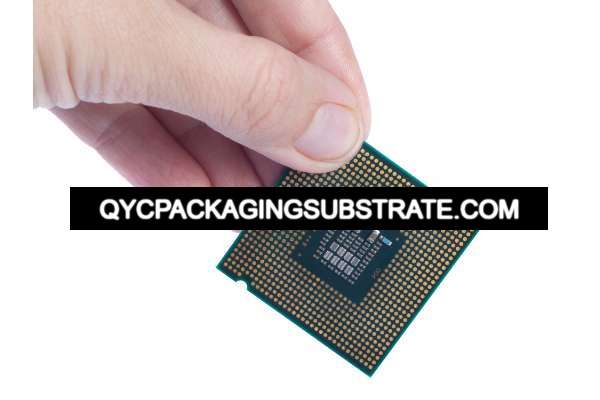
Advanced packaging substrate manufacturer. we can produce the best samllest bump pitch with 100um, the best smallest trace and spacing are 9um.
In contemporary PCB (Printed Circuit Board) engineering, an Advanced Packaging Substrate refers to an electronic packaging substrate that seamlessly integrates both rigid and flexible materials. The definition and distinctive characteristics of Advanced Packaging Substrates have gained paramount significance in the ongoing technological progression. Notably, continuous innovation and advancements in this domain have elevated the importance of advanced packaging substrates as a crucial component in fulfilling the requirements of modern high-performance electronics.
First, the definition of advanced packaging substrates in PCB engineering involves advancements in their structures and materials. The combination of traditional rigid substrates and flexible substrates gives advanced packaging substrates greater flexibility and plasticity. This special design allows for better adaptation to the extremely high space requirements of modern electronic equipment under the trend of miniaturization and lightweight.
Secondly, the special feature of advanced packaging substrates is also reflected in its significant improvement in the performance of electronic products. Compared with traditional substrates, the design of advanced packaging substrates is more advanced and complex, and can accommodate more devices and functional units, thus promoting the improvement of equipment performance. This highly integrated design makes advanced packaging substrates the first choice for areas such as smartphones, medical devices and communication systems.
Another special feature worth highlighting is the three-dimensional shape and foldability of the advanced packaging substrate. This makes it possible to achieve more complex and innovative designs within limited space.
Its definition in PCB engineering embodies a new concept of the fusion of rigid and flexible materials, and its special feature is that it provides more advanced design options and performance advantages for electronic products. Continuous innovation in this field provides electronic engineers with more tools and resources to meet growing market demands and technical challenges.
What types of advanced packaging substrates are there?
In contemporary electronics, advanced packaging substrates play a pivotal role in circuit design, offering versatility and enhanced performance across various application scenarios. Among these substrates, Ball Grid Array (BGA), Chip Scale Package (CSP), and System in Package (SiP) stand out, each presenting unique characteristics to cater to diverse design and manufacturing requirements.
Ball Grid Array (BGA) is a packaging technology known for its grid arrangement of spherical solder joints, providing a high solder joint count, efficient use of space, and superior electrical properties. This design makes BGA ideal for applications requiring dense connectivity and high reliability, and it is widely embraced in modern computers, communication equipment, and consumer electronics.
Chip Scale Package (CSP) stands out as a packaging technology tailored to closely align with the chip’s actual dimensions, creating a compact package. Renowned for its small size, lightweight design, cost-effectiveness, and excellent electrical performance, CSP proves highly beneficial in situations where factors like size, weight, and cost are pivotal considerations. Its advantages shine prominently in applications such as mobile devices, wireless sensors, and medical devices.
In summary, BGA and CSP, as advanced packaging substrates, provide the electronics industry with the flexibility to address specific design needs, offering improved performance and efficiency in a variety of electronic products.
It achieves a more compact and highly integrated electronic system by packaging multiple chips, capacitors, inductors and other components together. SiP is widely used in portable devices, IoT and wireless communication systems, providing these systems with a high degree of integration and superior performance.
Overall, the three advanced packaging substrate types, BGA, CSP and SiP, each play a unique role in the field of electronic design. BGA is suitable for scenarios that require high-density connections and reliability, CSP excels in applications with higher size and weight requirements, and SiP provides more advanced electronic system solutions through a high degree of integration. The continuous development and application of these advanced packaging substrates provide a solid foundation for the innovation and performance improvement of electronic products.
What are the advantages of advanced packaging substrates?
Advanced packaging substrates offer significant advantages in performance and design flexibility compared to traditional printed circuit boards (PCBs), providing PCB engineers with powerful tools and expanded application possibilities.
Primarily, the standout feature of advanced packaging substrates lies in their highly integrable design. Unlike traditional circuit boards, these substrates can accommodate multi-layer circuits more compactly, enabling a higher level of integration. This compact design facilitates the implementation of complex circuit structures in limited spaces, directly enhancing the performance potential of electronic products. This performance improvement is particularly impactful in mobile devices and high-end communication systems, influencing operating efficiency and response speed.
Additionally, sophisticated packaging substrates demonstrate exceptional design flexibility. Their composition integrates both rigid and flexible materials, enabling the adaptation to a wide range of intricate design specifications. This adaptability provides PCB engineers with the liberty to create circuit boards that seamlessly conform to the desired product shape, size, and performance criteria, liberating them from the limitations imposed by conventional rigid circuit boards. In the prevailing trend of developing lightweight and compact electronic products, this flexibility empowers designers to respond to market demands for innovation and distinctiveness.
In practical applications, advanced packaging substrates play a crucial role in embedded systems, wireless communications, medical equipment, and other fields. For example, in embedded systems, the performance advantages of these substrates contribute to higher computing power and stability, addressing the requirements of complex applications. In medical equipment, the design flexibility allows circuit boards to seamlessly adapt to the unique shapes and specifications of medical devices, thereby enhancing equipment reliability and stability.
In summary, the combined benefits of advanced packaging substrates in terms of performance and design flexibility provide PCB engineers with ample room for innovation. As technology advances, the widespread adoption of advanced packaging substrates in the electronics field is anticipated, promising more advanced and superior performance in future electronic products.
Why Choose Advanced Packaging Substrate Manufacturer?
In today’s rapidly evolving electronics landscape, choosing an advanced packaging substrate manufacturer offers unique advantages over other options, which involves a deep understanding of technology, experience and expertise. Here’s a closer look at why, among many options, specialized manufacturers of advanced packaging substrates are the most popular.
Certainly, let’s rephrase the provided passage:
Initially, adept manufacturers enjoy notable technological advantages. The ever-evolving landscape of electronic technology has led to increased complexities in the development and production of advanced packaging substrates. Leveraging continuous research and technological progress, these skilled manufacturers can keep pace with the latest industry trends. This commitment ensures that their products adhere to the most up-to-date technical standards, providing customers with access to innovative solutions tailored to dynamic market demands.
Secondly, seasoned manufacturers play a crucial role in offering essential support, particularly in intricate designs and challenging application scenarios. Electronic product design often necessitates achieving more functions and higher performance within limited spatial constraints. Leveraging years of accumulated experience, professional manufacturers can assist customers in optimizing designs and ensuring optimal product performance. Their familiarity with a diverse range of advanced packaging technologies enables them to provide practical solutions that address challenges, ultimately ensuring the successful launch of products.
In addition, the expertise of professional manufacturers is particularly outstanding in material selection, process control and quality assurance. The manufacturing of advanced packaging substrates involves multiple levels of complex processes, including material selection, interlayer connection design, blind hole drilling, metallization and other steps. Professional manufacturers can ensure that every aspect is precisely controlled to ensure the performance and reliability of the final product.
In addition, professional manufacturers usually have established a complete quality management system to ensure product quality through strict quality inspection processes. In demanding applications, product quality is crucial. Professional manufacturers provide high-quality advanced packaging substrates through strict quality control, reducing the risks that customers may face during the product life cycle.
In general, choosing a professional advanced packaging substrate manufacturer not only means gaining technological leadership, but also means gaining the support of rich experience and comprehensive professional knowledge. This will help customers succeed in a highly competitive market, ensuring their products lead in performance, reliability and innovation.
packaging substrates
What is the manufacturing process for advanced packaging substrates?
The production of advanced packaging substrates is a highly intricate and complex process that entails skillfully integrating various layers of both rigid and flexible materials. Each step, from the creation of the motherboard to the substrate, demands meticulous precision and stringent process control to guarantee that the ultimate product not only meets but exceeds industry standards in terms of performance and reliability.
Design and layout
The first step in manufacturing advanced packaging substrates is precise design and layout. This stage involves key steps such as circuit graphics planning, wiring, and component placement. Design engineers need to consider the overall structure, especially the connection between Motherboard and Substrate and the three-dimensional shape requirements.
Material selection
When manufacturing advanced packaging substrates, material selection is critical. Different applications require different types of materials, including rigid and flexible substrates, conductive and insulating layers, and more. These materials must meet performance requirements and perform well throughout the manufacturing process.
Preparing Motherboard
Motherboard is the core part of advanced packaging substrates and carries the main functions of circuits. In this step, multiple layers of rigid substrates are stacked and passed through a series of processes, including chemical etching, blind hole drilling, etc., to form the basic structure of the Motherboard. This process requires a high degree of manufacturing precision to ensure the accuracy and reliability of the circuit.
Prepare Substrate
Substrate is the key piece connecting Motherboard and other components. During this manufacturing stage, flexible substrates are added to the structure, adding flexibility and bendability to advanced packaging substrates. Special process control ensures the quality of the combination of rigidity and softness to meet the three-dimensional shape requirements of the design.
Interlayer connections and metallization
After the preparation of Motherboard and Substrate is completed, the next step is to connect the layers. This step involves how the circuits are connected, usually through special metallization. This not only requires a high degree of precision, but also ensures connection reliability and conductivity.
Final assembly and testing
At the end of the manufacturing process, advanced packaging substrates enter final assembly and testing stages. This includes components installation, soldering and other steps, as well as a series of tests to ensure the normal operation of each component and connection.
Even the slightest manufacturing error has the potential to result in circuit failure, underscoring the indispensability of precision and process control. Rigorous manufacturing protocols are imperative to guarantee optimal product functionality in challenging applications, meeting the stringent performance and reliability standards inherent in today’s electronic products.
In what areas are advanced packaging substrates widely used?
Advanced packaging substrates, owing to their outstanding performance and adaptability, have garnered widespread applications across diverse sectors, overcoming the constraints of traditional circuit boards and revitalizing numerous high-tech products. Beyond their prevalent use in smartphones, medical devices, and aerospace systems, advanced packaging substrates exhibit significant potential in various emerging areas:
Electric Vehicles and Transportation
The surge in electric vehicles and the evolution of intelligent transportation have elevated the expectations for electronic systems. Advanced packaging substrates emerge as a solution that offers compactness, light weight, and high performance for electric vehicle control systems. This facilitates substantial advancements in energy efficiency, driving experience, and overall reliability of electric vehicles. Furthermore, in traffic monitoring systems, the flexibility and integrability of advanced packaging substrates position them as pivotal components in the development of smart transportation solutions.
Automated industry
In the realm of industrial automation, the utilization of advanced packaging substrates proves instrumental in enhancing control systems, sensors, and communication equipment to elevate production efficiency, curtail energy consumption, and facilitate intelligent manufacturing. These substrates boast bendability and three-dimensional shape design, rendering them adaptable to the spatial constraints of diverse industrial equipment. Consequently, they offer robust support for the digital transformation of various factories and production lines.
The synergy between advanced packaging substrates and the Internet of Things (IoT) and Edge Computing is pivotal. These substrates play a central role in interconnecting a plethora of IoT devices and bolstering edge computing capabilities. With their compact design, they are well-suited for embedded systems and sensor networks, enabling real-time data processing and analysis. This, in turn, ensures heightened performance and reliability in IoT applications.
Emerging medical technologies
In addition to traditional medical device applications, advanced packaging substrates also show great potential in emerging medical technology fields. For example, in the fields of wearable medical devices, remote medical monitoring systems and smart medical devices, advanced packaging substrates can provide highly integrated solutions for these devices to achieve more portable and intelligent medical services.
Smart Home and Consumer Electronics
The growing expansion of the smart home and consumer electronics markets underscores the rising significance of advanced packaging substrates in these domains. These substrates play a crucial role in various applications, ranging from smart home control systems to high-performance audio and video equipment. Their design flexibility and customizability make them essential in catering to diverse consumer needs, ultimately enhancing home life with smarter and more convenient experiences.
It is providing strong support for innovation and progress in different industries. As technology continues to advance, we have reason to expect that advanced packaging substrates will continue to promote the development of science and technology and bring more surprises and possibilities to various fields.
How to find a professional advanced packaging substrate manufacturer?
In the rapidly evolving landscape of electronic technology, the careful selection of a proficient advanced packaging substrate manufacturer is paramount to the success of any project. Navigating through numerous manufacturers, the task at hand for PCB engineers and enterprises is to discern and establish effective collaborative relationships wisely.
To begin with, the choice of an appropriate advanced packaging substrate manufacturer necessitates a comprehensive understanding of their technical prowess and experience. Industry leaders typically boast extensive manufacturing backgrounds, stay abreast of the latest technological trends, and allocate substantial resources towards research and development. Delving into a manufacturer’s history and appraising their success stories in advanced packaging substrates serves as a solid foundation for making an informed selection.
Equally critical is the evaluation of a manufacturer’s production capabilities and equipment proficiency. Given the intricate processes involved in advanced packaging substrate manufacturing, it is imperative to ensure that the chosen manufacturer possesses advanced, reliable equipment and exhibits a high level of production competence. This is pivotal in guaranteeing the quality and stability of the final product.
While assessing a manufacturer, attention should extend beyond technical capabilities to encompass soft power aspects. The professionalism of the manufacturer’s team, service levels, and their ability to comprehend customer needs become focal points of scrutiny. Manufacturers offering high-level technical support and considerate after-sales service contribute significantly by providing timely assistance and guidance throughout the project lifecycle.
Strategically, forging partnerships with industry-leading suppliers holds significance. Such manufacturers are adept at staying attuned to industry trends, offering customers forward-looking and innovative solutions. Collaboration with these manufacturers can confer technical advantages, expedite time to market, and enhance market competitiveness.
Moreover, industry-leading manufacturers typically maintain strong relationships with material suppliers, technology partners, etc. This network allows them to access competitive prices and higher quality raw materials, effectively managing production costs and enhancing product cost-effectiveness.
In the selection process, adherence to relevant quality certification standards is also crucial. Manufacturers with certifications such as ISO and UL often deliver more reliable and stable products, instilling confidence in the quality of their offerings.
In conclusion, the selection of a professional advanced packaging substrate manufacturer necessitates a holistic consideration of factors encompassing technical and soft power, cooperative relationships, and adherence to quality standards. Establishing robust partnerships with industry leaders provides vital support for project success, ensuring products secure a favorable position in the market. For PCB engineers, the meticulous choice of a reliable manufacturer stands as a pivotal step towards project success.
What do advanced packaging substrate manufacturers quote?
When selecting an advanced packaging substrate manufacturer, accurate quotation is one of the keys to ensuring project success. Understanding and considering various quote factors can provide high-quality products within budget. Here are some key factors to note during this process:
The Importance of Quotation Factors
Material selection for advanced packaging substrates is a crucial aspect influenced by cost-performance trade-offs, with manufacturers providing quotes based on varying material costs. The decision hinges on achieving a balance between economic considerations and desired performance. It’s imperative to thoroughly assess a manufacturer’s material supply chain reliability and the quality of materials employed.
Evaluating the advancement and stability of a manufacturer’s processes is essential, ensuring they align with project requirements. An understanding of the manufacturer’s workmanship level becomes paramount to guarantee the successful realization of project objectives.
Delivery Time: Time is an important factor in project success. In the quote, the manufacturer usually provides an estimate of delivery time. For time-sensitive projects, it is necessary to communicate with the manufacturer and ensure that it can complete production within the scheduled time.
How to ensure that the budget and quality of the project meet expectations?
Transparent communication: Maintaining transparent communication with manufacturers is key to ensuring budget and quality goals are met. Clearly communicate project needs, budget constraints, and quality expectations so manufacturers can provide accurate quotes.
Sample verification: Before formal production, requiring manufacturers to provide samples for verification is an effective way to ensure quality. By inspecting samples, manufacturing capabilities and product quality can be assessed to ensure they meet project standards.
Evaluating the quality of a manufacturer’s products hinges on a thorough understanding of their quality management system. Key indicators include ISO certification and the presence of robust quality control processes. Prior to entering into a contractual agreement, a meticulous review of contract details is crucial to preempt potential issues. It is imperative that the contract encompasses all quotation specifics such as materials, workmanship, and delivery time, while clearly outlining the division of responsibilities. When selecting an advanced packaging substrate manufacturer, a comprehensive grasp of the factors influencing a quote, coupled with proactive communication and effective project management, ensures the delivery of a high-quality product within budget. This holistic approach not only facilitates the successful project implementation but also lays the foundation for a long-term and stable collaborative relationship.
Package Substrate FAQs
What is a Package Substrate?
A Package Substrate is an advanced electronic packaging board that combines rigid and flexible materials, providing excellent performance in space-constrained or three-dimensional applications.
Why choose Package Substrate over other boards?
Compared to traditional boards, Package Substrates provide enhanced flexibility and adaptability to complex designs. Their three-dimensional shape and foldable nature make them competitive in miniaturization and lightweight applications.
How are Package Substrates manufactured?
The manufacturing process involves layering rigid and flexible base materials, preparing circuit patterns, chemical etching, blind via drilling, and other precision steps. Strict process control ensures the final product’s performance and reliability.
What are the applications of Package Substrates?
Package Substrates find wide-ranging applications in electronic devices such as smartphones, medical monitoring equipment, aerospace systems, and other areas where space efficiency and performance are critical.
How do I get a quote for Package Substrates?
Obtaining a quote involves considering factors such as material selection, manufacturing processes, and customization requirements. Thorough analysis of the quote helps ensure that project budgets and quality expectations are met.
What are common FAQs about Package Substrates?
Common questions include inquiries about performance, design considerations, and costs associated with Package Substrates. Addressing these FAQs provides a comprehensive understanding for engineers and designers.
Exploring these frequently asked questions provides valuable insights into the world of Package Substrates, aiding professionals in making informed decisions for their PCB designs and applications.