 Professional Flip-Chip Packaging Substrate Supplier

Embedded IC PCB manufacturing. Open Embedded cavity PCBs, the PCBs will be made with cavities, open cavity on the top layer or bottom layer. or in the Middle of each layer. we called it buried cavity PCBs. We can use high frequency and high speed or ceramic materials for production.
In modern electronics, printed circuit boards (PCBs) are the backbone of countless devices, enabling seamless integration of electronic components. Among the many applications of PCBs, embedded IC PCB manufacturing has become a transformative technology that has completely changed the way electronic systems are designed and manufactured. In this comprehensive guide, we take a deep dive into the complexities of embedded IC PCB manufacturing, exploring its importance, design principles, manufacturing processes, cost factors, material considerations, key manufacturers, and quality customers in this dynamic industry The core essence of service.
What is embedded IC PCB manufacturing?
Embedded IC PCB manufacturing is an advanced electronic manufacturing technology that embeds integrated circuits (ICs) directly into a Printed Circuit Board (PCB) substrate without the need for traditional discrete IC packaging. This innovative approach has attracted widespread attention in the electronics industry and has demonstrated significant advantages in a variety of applications.
First, embedded IC PCB manufacturing can significantly reduce the size and volume of the circuit board. Traditional IC packaging requires extra space to accommodate the IC chip, while embedded IC PCB can directly integrate the IC into the PCB substrate, so the space can be used more efficiently, making electronic devices more compact and lightweight. This is particularly important for portable devices and embedded systems, which often require the smallest possible size.
Secondly, embedded IC PCB manufacturing can improve the performance and reliability of circuits. Since the IC is directly embedded into the PCB substrate, the electrical characteristics of the circuit are improved and the signal transmission is more stable and reliable. In addition, compared with traditional packaging, embedded IC PCB has lower resistance, inductance and crosstalk, which can reduce signal attenuation and interference and improve system performance and anti-interference capabilities.
In addition, embedded IC PCB manufacturing can also reduce costs and improve production efficiency. Traditional IC packaging requires additional materials and processes for packaging and packaging testing, while embedded IC PCB manufacturing can simplify the manufacturing process and reduce production costs and cycles. In addition, because embedded IC PCB can integrate multiple functional modules and components more easily, the assembly cost and complexity of the overall system can be reduced.
Finally, embedded IC PCB manufacturing is also more environmentally friendly. Since embedded IC PCBs can reduce the size and material usage of electronic devices, resource consumption and waste generation can be reduced. In addition, because embedded IC PCB can improve the performance and reliability of the circuit, it can extend the service life of the device and reduce the generation of electronic waste.
In summary, embedded IC PCB manufacturing is an advanced technology with broad application prospects. It can not only significantly improve the performance and reliability of electronic equipment, but also reduce costs, improve production efficiency, and is environmentally friendly. One of the important directions for the future development of electronic manufacturing industry.
Embedded IC PCB
How to design embedded IC PCB?
Designing embedded IC PCB is a job that requires highly professional skills and precise control of details. During this process, engineers must not only consider the functional and performance requirements of the circuit design, but also fully understand and follow the basic principles of PCB design. Here are some key aspects that engineers need to pay special attention to when designing embedded IC PCBs:
First, engineers must have a deep understanding of the circuit’s functional requirements and system performance metrics. This includes understanding the functions and specifications of each embedded IC, as well as how the entire circuit system works. Only by fully understanding how the circuit works can we effectively design an embedded IC PCB that meets the requirements.
Second, engineers need to accurately lay out circuit components and wires. By leveraging advanced PCB design software, engineers can lay out circuits to maximize signal routing, power distribution and thermal management. This includes determining where to place embedded ICs, designing the board hierarchy, and planning the routing of signal lines to minimize signal interference and power loss.
Additionally, engineers need to consider the physical layout and size constraints of the circuit board. Embedded IC PCBs usually need to accommodate multiple ICs and other electronic components in a limited space, so the location and layout of components must be reasonably arranged during the design process to ensure the compactness and efficiency of the entire circuit board.
In addition, thermal management is also an aspect that requires special attention when designing embedded IC PCBs. Since integrated circuits generate heat during operation, engineers must design an effective heat dissipation system to ensure that the embedded IC PCB can maintain a stable temperature when working for a long time. This includes designing heat sinks, fans or thermal paths, and selecting appropriate heat dissipation materials and methods.
Finally, engineers also need to consider the feasibility of manufacturing and assembly when designing embedded IC PCBs. This includes selecting suitable PCB materials and processes, as well as designing a board layout that is easy to produce and assemble. By taking manufacturing and assembly requirements into account during the design phase, later production costs and engineering risks can be effectively reduced.
To sum up, designing embedded IC PCB requires engineers to fully understand the circuit functions and performance requirements and follow professional design principles. Through precise layout, effective signal routing, proper thermal management and considering the feasibility of manufacturing assembly, engineers can design embedded IC PCBs with high performance, reliability and cost-effectiveness.
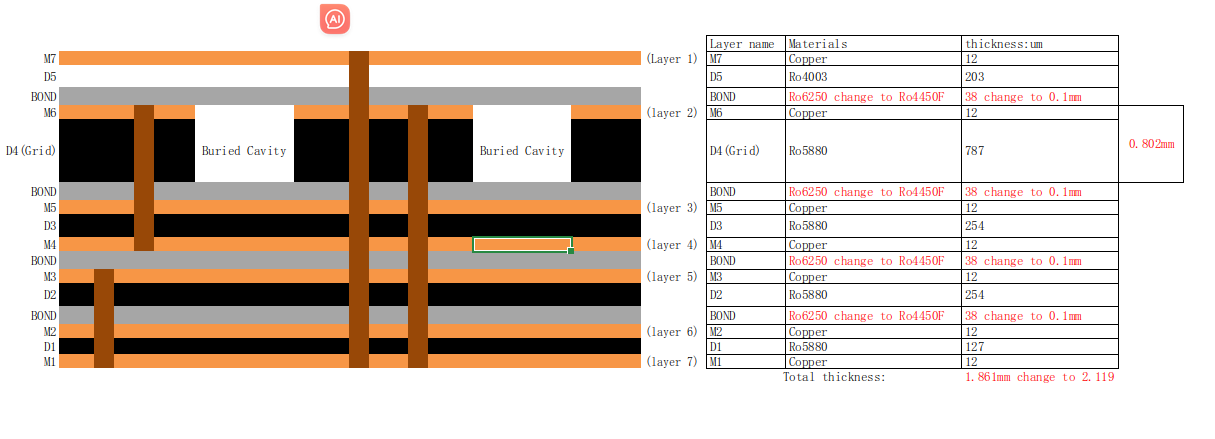
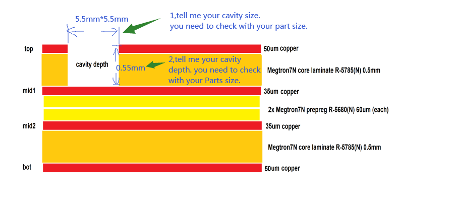
Buried Cavity PCBs
What is the manufacturing process of embedded IC PCB?
The manufacturing process of embedded IC PCB is a complex and precise process, aiming to achieve the close integration of integrated circuits and PCB substrates, thereby creating high-performance, high-reliability electronic systems. This process typically involves multiple key stages, each of which must be carefully planned and executed to ensure that the final product is of the desired level of quality and performance.
First, the process of manufacturing embedded IC PCB begins with the substrate preparation stage. At this stage, selecting a suitable substrate material is crucial. Commonly used substrate materials include FR-4, Rogers, and ceramics. Each material has different properties, such as thermal conductivity, dielectric constant, and mechanical strength. Manufacturers select the most appropriate substrate material based on the needs of specific applications, and perform the necessary processing and preparation work to ensure the flatness and surface quality of the substrate.
Next comes the lamination stage, which is one of the key steps in building the embedded IC PCB structure. During the lamination process, manufacturers stack multi-layer substrates and dielectric layers according to design requirements, and achieve electrical connections between layers through inter-layer connections (such as blind vias and buried vias). This process requires precise control and adjustment to ensure the alignment between the layers and the accuracy of the gaps between layers, thereby laying the foundation for subsequent circuit patterning and IC integration.
This is followed by the circuit patterning stage, where manufacturers use photolithography technology to transfer the designed circuit pattern to the substrate surface. This process involves steps such as photoresist coating, exposure, development and etching. Through precise control and adjustment, the circuit pattern is accurately transferred to the substrate surface, providing a reliable foundation for subsequent IC integration and connection.
IC integration is one of the key links in manufacturing embedded IC PCB. At this stage, manufacturers utilize advanced IC packaging and connection technologies to integrate IC chips directly onto the substrate surface. The IC chip is connected to the circuit pattern through soldering, gold wire connection or ball grid array, and the electrical connection is achieved through conductive adhesive or laying lines. This process requires a high degree of precision and stability to ensure perfect integration and stable operation of the IC chip and substrate.
The last is the surface treatment stage, where manufacturers perform surface coating and treatment on embedded IC PCBs to protect circuit patterns and IC chips, and improve their environmental resistance and corrosion resistance. Commonly used surface treatment methods include spray plating, tin spray, gold spray, silver spray, etc. These treatment methods can effectively prevent oxidation, pollution and mechanical damage, and ensure the long-term stability and reliability of embedded IC PCBs.
In summary, the manufacturing process of embedded IC PCB is a highly technical and complex task, which requires manufacturers to have rich experience and superb technology to ensure that each step can be accurately executed to achieve embedded Seamless integration and functionality of style components.
What are the cost considerations for embedded IC PCBs?
The cost of embedded IC PCB is one of the important factors that needs to be carefully considered during the manufacturing process. Its cost is affected by many factors, including design complexity, material selection, manufacturing technology and volume requirements.
First, design complexity is one of the key factors affecting the cost of embedded IC PCBs. Complex designs require more engineering resources and time to complete, increasing the cost of the design phase. For example, requirements for high-density layout and complex signal routing may require more layers and higher-level design techniques, which will further increase costs.
Secondly, material selection also has a direct impact on cost. Different types of substrate materials have different cost and performance characteristics. For example, high-frequency applications often require the use of more expensive specialty materials such as Rogers or PTFE, while for general applications the lower-cost FR-4 material may be chosen.
Manufacturing technology is also an important factor in determining cost. Adopting advanced manufacturing technologies often increases manufacturing costs, but may also lead to higher performance and better quality control. For example, the use of high-precision processes and advanced automation equipment can improve production efficiency, but the investment costs of these equipment and technologies will also increase manufacturing costs.
Finally, volume demand is one of the key factors affecting costs. High-volume production often reduces unit costs because fixed costs can be spread over more products. However, in the early stages, smaller production volumes may result in higher unit costs because there are relatively few fixed costs to amortize.
Although embedded IC technology may come with a higher upfront cost, over the long term it often delivers long-term benefits in performance and reliability that often outweigh the initial investment. By increasing integration and reducing connection points, embedded IC PCBs can improve system stability and reliability, reducing maintenance and troubleshooting costs. Therefore, while the initial cost may be higher, embedded IC PCBs are often viewed as an attractive investment given their long-term advantages.
What materials are used in embedded IC PCB?
As a key component in modern electronic equipment, the performance and reliability of embedded IC PCB are often directly affected by the selected materials. In order to meet the needs of different applications and working conditions, manufacturers usually choose various materials as the substrate for embedded IC PCBs. The following will introduce several common embedded IC PCB materials and their characteristics.
First is the FR-4 substrate, which is one of the most common PCB substrate materials. The FR-4 substrate is composed of glass fiber and epoxy resin and has excellent insulation properties, high temperature resistance and mechanical strength. The material’s characteristics make it suitable for a variety of general applications such as consumer electronics, communications equipment and industrial control systems.
Next is the Rogers substrate, which is a high-performance dielectric substrate commonly used in applications requiring higher frequencies and lower losses. The Rogers substrate uses ceramic-filled PTFE (polytetrafluoroethylene) as the dielectric, which has excellent dielectric properties and signal transmission characteristics. This material is commonly used in radar systems, microwave communications equipment and high-frequency RF applications.
In addition, ceramic substrate is another common embedded IC PCB material. Ceramic substrates have excellent high-frequency characteristics, high temperature resistance and chemical stability, making them suitable for applications requiring extremely high performance and reliability. Due to their excellent properties, ceramic substrates are often used in high-end electronic equipment in aerospace, medical equipment and military fields.
In general, different embedded IC PCB materials have their own unique characteristics and scope of application. Choosing the right material depends on design needs, performance requirements and working environment, and manufacturers need to make comprehensive considerations and choices based on specific circumstances. By rationally selecting materials and combining them with high-quality manufacturing processes, embedded IC PCBs can be ensured to achieve optimal performance and reliability in various application scenarios.
Where are embedded IC PCBs manufactured?
In the embedded IC PCB manufacturing process, the choice of manufacturing location has an important impact on product quality, delivery time and cost-effectiveness. For our company, the key to manufacturing embedded IC PCBs is to ensure that the right manufacturer is selected and produced at the right location.
When our company is looking for manufacturers, we will give priority to those with advanced equipment and technology, strict quality control standards and rich experience. Such manufacturers can guarantee product quality and stability, and can flexibly respond to various production needs.
When selecting a manufacturing location, we typically consider production costs, ease of transportation, and the manufacturer’s geographic location. We tend to choose locations close to the supply chain, which helps shorten lead times and reduce shipping costs. Additionally, choosing a conveniently located manufacturing location can reduce potential shipping risks and delays.
For embedded IC PCB manufacturing, the Asian region is often an ideal choice. Asia has abundant electronic manufacturing resources and technical talents, as well as a complete supply chain network. In particular, places such as China, Taiwan, South Korea and Japan have many professional PCB manufacturers providing various advanced manufacturing services.
Therefore, our company usually chooses manufacturers in Asia for the production of embedded IC PCBs. We have established long-term relationships with these manufacturers and work together to advance embedded technology and ensure our products are successful in the market.
What are the characteristics of great customer service?
In the embedded IC PCB manufacturing industry, quality customer service is key to ensuring customer satisfaction and building long-term relationships. It is not only a guarantee of product quality and delivery time, but also a proactive attitude towards communication and problem-solving. Below we’ll dive into a few key attributes of great customer service:
The first is responsiveness. Excellent customer service means a manufacturer is responsive to customer needs and questions in a timely manner. Whether it is inquiries about order status or technical questions, customers hope to receive timely feedback and solutions. Therefore, responding to customer needs in a timely and effective manner is an important part of ensuring customer satisfaction.
Second is transparency. Transparency is crucial in communicating with customers. Manufacturers should provide clear order tracking information, promptly update customers on the progress of their orders, and promptly communicate any potential issues or delays. Through transparent communication, manufacturers can enhance customer trust and build strong relationships.
Expertise is another important trait. Customers want to work with manufacturers who understand their needs and can provide professional advice. In the field of embedded IC PCB manufacturing, the technical complexity is high, so manufacturers must have sufficient expertise to ensure that customer needs are best met.
Reliability is the cornerstone of great customer service. Manufacturers must keep their promises and deliver high-quality products on time. Customers rely on the stability and reliability of manufacturers, so manufacturers must maintain high standards, both in terms of product quality and delivery times.
Finally, there is a commitment to customer satisfaction. Excellent customer service is not just about meeting customer needs, but more importantly, ensuring customer satisfaction. Manufacturers should actively seek customer feedback and continuously improve and enhance service quality to ensure that customer needs are fully met.
Overall, in the embedded IC PCB manufacturing industry, excellent customer service is the key to a successful relationship between manufacturers and customers. Through prompt response, transparent communication, expert knowledge, reliable delivery and commitment to customer satisfaction, manufacturers can ensure customer satisfaction and promote mutual success.
Frequently Asked Questions
What are the primary benefits of Embedded IC PCBs?
Embedded IC PCBs offer several key advantages over traditional PCBs. Firstly, they enable significant miniaturization of electronic devices by integrating ICs directly into the PCB substrate, thereby reducing overall form factor and footprint. Secondly, Embedded IC technology enhances signal integrity and reduces electromagnetic interference (EMI) by minimizing trace lengths and optimizing signal paths. Additionally, Embedded ICs improve thermal management by facilitating direct heat dissipation through the PCB substrate, leading to enhanced reliability and performance of electronic systems.
How does Embedded IC technology impact PCB form factor?
Embedded IC technology revolutionizes PCB design by eliminating the need for discrete IC packaging, thus enabling more compact and streamlined PCB layouts. By integrating ICs directly into the PCB substrate, Embedded ICs contribute to the reduction of overall board size and thickness, allowing for the development of smaller, lighter, and more sophisticated electronic devices. This reduction in form factor is particularly advantageous in applications where space constraints and weight considerations are critical, such as mobile devices, wearables, and IoT sensors.
What are the challenges associated with designing Embedded IC PCBs?
Designing Embedded IC PCBs presents several unique challenges that engineers must address. One major challenge is ensuring proper heat dissipation and thermal management, as embedding ICs directly into the PCB substrate can increase localized heat generation. Engineers must employ effective thermal design strategies, such as incorporating thermal vias, copper planes, and heatsinks, to dissipate heat and prevent overheating of embedded components. Additionally, designing for manufacturability and reliability requires careful consideration of substrate materials, assembly processes, and signal integrity to ensure successful integration and optimal performance of Embedded ICs.
How can manufacturers ensure the reliability of embedded components?
Ensuring the reliability of embedded components in PCBs requires stringent quality control measures and adherence to industry standards. Manufacturers must carefully select high-quality substrate materials with suitable thermal and mechanical properties to withstand the stresses of IC integration and thermal cycling. Additionally, advanced manufacturing techniques, such as precision assembly processes and thorough testing procedures, are essential to verify the integrity and functionality of embedded components before deployment. By prioritizing quality assurance and reliability testing throughout the manufacturing process, manufacturers can guarantee the long-term performance and durability of Embedded IC PCBs.