 Professional Flip-Chip Packaging Substrate Supplier

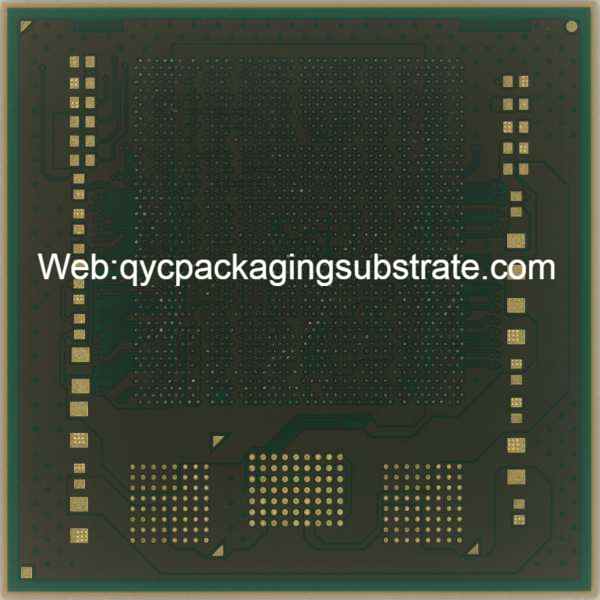
What is FCBGA Package Substrate?
Advanced FCBGA package Substrate manufacturing. High multilayer Packaging substrate manufacturer. the smallest via holes size are 50um. the smallest trace and Spacing are 10um/10um.
FCBGA Package Substrate, as an important advanced packaging technology in the field of modern electronics, plays a vital role in high-performance electronic devices with its unique characteristics. One of the core features of this packaging technology is the use of Flip-Chip technology, which cleverly flips the chip over and mounts it on the substrate, and realizes circuit connection through ball solder joints. This innovative design provides a more compact and efficient solution for electronic equipment.
The use of Flip-Chip technology enables FCBGA Package Substrate to have excellent performance in connecting circuits. Through the precise layout of ball solder joints, the packaging substrate can achieve more connection points in a small space, thereby enhancing the conductivity and reliability of the circuit. This connection method not only improves the overall performance of electronic devices, but also provides the possibility for higher-density integrated circuits.
In practical applications, FCBGA Package Substrate has been widely used in high-performance electronic equipment. Its packaging method provides excellent protection for modern chips while enabling efficient heat dissipation of the chip. This makes FCBGA Package Substrate especially suitable for scenarios that have strict requirements on stability and heat dissipation performance, such as computer servers, communication equipment and other fields. Its application in core components such as high-performance processors and graphics processing units has effectively improved the overall performance level of electronic equipment.
The advancement of FCBGA Package Substrate is not only reflected in its packaging method, but also involves many different types of technologies. By using different levels of HDI technology, Substrate-like PCB (SLP), etc., FCBGA Package Substrate can better meet the specific needs of electronic equipment in different fields. This flexibility makes FCBGA Package Substrate an ideal choice to meet the needs of different application scenarios.
Overall, FCBGA Package Substrate, as an advanced packaging technology, has successfully found wide applications in high-performance electronic equipment through its design using Flip-Chip technology and ball solder joint connection circuits. It not only improves the connection efficiency of the circuit, but also injects new vitality into the overall performance and stability of electronic equipment. In the field of electronic engineering, FCBGA Package Substrate is undoubtedly one of the key factors driving the continuous advancement of technology.
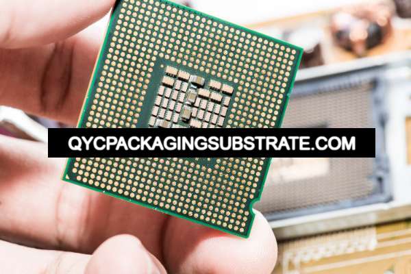
FCBGA package Substrate
What functions does FCBGA Package Substrate have?
FCBGA Package Substrate (Flip-Chip Ball Grid Array packaging substrate), as an advanced packaging technology, plays a vital role in the field of electronic engineering. Its main functions cover several key aspects, among which electrical connections, mechanical support and chip cooling are its unique features.
First, FCBGA Package Substrate excels at electrical connections. Using Flip-Chip technology, this packaging method flip-chips the chip onto the substrate through ball solder joints. This design greatly increases the connection density of the circuit, allowing more connection points to be implemented in a limited space. As the transmission rate of electrical signals and the demand for data communication continue to increase, FCBGA Package Substrate has become an ideal choice in modern high-performance electronic equipment with its excellent electrical connection performance.
Secondly, FCBGA Package Substrate provides excellent mechanical support. The substrate is designed not only for electrical connections, but also for solid support of the chip. This mechanical support helps prevent the chip from being displaced or damaged during use, especially if the device is subject to external shock or vibration. By ensuring solid mechanical support, FCBGA Package Substrate effectively increases the stability and reliability of electronic devices.
Another key function is heat dissipation of the chip. As chip power density increases, heat dissipation becomes critical. Through its design, FCBGA Package Substrate directly connects the chip to the substrate, allowing heat to be conducted to the substrate more efficiently. In addition, by arranging heat dissipation structures on the substrate, such as heat dissipation holes and heat dissipation layers, FCBGA Package Substrate can more effectively transfer heat to the surrounding environment to ensure that the chip operates within a suitable temperature range.
Taken together, the multiple functions of FCBGA Package Substrate in terms of electrical connection, mechanical support, and chip heat dissipation make it an indispensable key technology in current electronic engineering. By increasing connection density, ensuring mechanical stability and achieving effective heat dissipation, FCBGA Package Substrate provides reliable solutions for the design and manufacturing of modern high-performance electronic devices, promoting the continuous innovation and development of electronic technology.
What are the different types of FCBGA Package Substrate?
As an important part of electronic engineering, FCBGA Package Substrate has been derived into various types to meet various needs driven by different applications and technological advances. Among them, different levels of HDI technology and Substrate-like PCB (SLP) are areas that have attracted much attention.
First of all, High-Density Interconnect (HDI) technology plays a key role in the evolution of FCBGA Package Substrate. HDI technology enables higher performance and smaller package size by increasing connection density at different levels. Different levels of this technology include Microvia and Build-up levels. Through the ingenious design of these levels, FCBGA Package Substrate exhibits excellent performance in high-density wiring and signal transmission.
In addition, Substrate-like PCB (SLP), as an innovative form of FCBGA Package Substrate, provides more flexible design options for electronic devices. Compared with traditional Rigid PCB, SLP is thinner, lighter, and higher-density, and can meet more complex wiring requirements. The special structure of SLP gives it obvious advantages in miniaturized equipment and high-performance computing applications.
HDI technology and SLP have their own characteristics in the application of FCBGA Package Substrate. HDI technology focuses more on improving connection density and performance, and is suitable for scenarios with more demanding requirements for high integration, such as high-performance computing and communication equipment. Relatively speaking, SLP focuses more on realizing more functions in a limited space, and is suitable for fields such as portable devices and embedded systems.
These different types of FCBGA Package Substrate not only meet specific application needs, but also provide electronic engineers with more choices and room for innovation. Choosing an applicable FCBGA Package Substrate among different types can better balance performance, package size and wiring requirements, providing a more flexible solution for device design. Therefore, understanding these different types of FCBGA Package Substrate is crucial for practitioners in the field of electronic engineering.
What is the relationship between FCBGA Package Substrate and IC packaging?
FCBGA Package Substrate (Flip-Chip Ball Grid Array Package Substrate) plays a vital role in electronic engineering, especially in fields related to IC packaging. First, we need to understand the classification of chip packaging technologies and their close connection with FCBGA Package Substrate.
The classification of chip packaging technology mainly involves the method of chip connection and the design of the packaging structure. Among them, FCBGA Package Substrate uses Flip-Chip technology, which is an advanced packaging method. Flip-Chip technology flips the chip over and installs it on the substrate, and realizes the connection between the chip and the substrate through small spherical solder joints. Compared with traditional packaging technologies, such as Wire Bonding, this method has higher density and shorter signal transmission paths, thereby improving circuit performance.
Chip packaging technologies related to FCBGA Package Substrate mainly include Ball Grid Array (BGA), Quad Flat Package (QFP), etc. BGA is a common chip packaging method, and FCBGA is an evolved form that uses Flip-Chip technology to make the connection tighter and more efficient. QFP is a traditional packaging method, which is different from FCBGA in connection method and performance.
FCBGA package Substrate
In IC packaging, FCBGA Package Substrate closely combines the chip with the substrate through its unique design to form a compact and highly integrated unit. This connection method not only improves the integration of the circuit, but also improves the efficiency of signal transmission. At the same time, the structure of FCBGA Package Substrate also takes into account the needs for heat dissipation, providing a good environment for the stable operation of the chip.
The relationship between FCBGA Package Substrate and IC packaging is reflected in their joint promotion of the development of electronic engineering. By adopting advanced chip packaging technology, especially FCBGA Package Substrate, we are able to make significant progress in miniaturized, high-performance electronic devices. This interrelated relationship not only promotes continuous innovation in packaging technology, but also promotes the development of the entire electronics industry. In the era of rapid technological change, the in-depth cooperation between FCBGA Package Substrate and IC packaging will provide more reliable and advanced solutions for the design and manufacturing of future electronic equipment.
What is the difference between FCBGA Package Substrate and traditional PCB?
Compared with traditional PCB (Printed Circuit Board, printed circuit board), FCBGA Package Substrate (Flip-Chip Ball Grid Array package substrate) shows unique characteristics and wide range of applications. Among electronic devices such as Motherboard, the uniqueness of FCBGA Package Substrate is mainly reflected in the following aspects.
First, FCBGA Package Substrate uses Flip-Chip technology to flip the chip and install it on the substrate, and realize circuit connection through ball solder joints. This packaging method is more advanced than the traditional PCB installation method and helps improve the performance and stability of the circuit. Traditional PCBs usually use surface mount technology (SMT), and FCBGA Package Substrate’s Flip-Chip design makes the circuit more compact and provides more connection points, thereby increasing the integration of the circuit.
In terms of application in Motherboard, FCBGA Package Substrate is widely used in the packaging of integrated circuits.Compared with traditional PCB, FCBGA Package Substrate can better adapt to high-density and high-performance requirements and provide better performance for electronic devices.
In addition, FCBGA Package Substrate is accompanied by other advanced packaging technologies, such as Substrate-like PCB (SLP) and High-Density Interconnect (HDI) Substrate. The application of these technologies makes the overall electronic design more flexible and efficient. SLP technology allows designers to implement more functions in a limited space, while HDI Substrate further enhances the performance and reliability of the circuit by increasing the circuit density of the circuit board.
Overall, the application of FCBGA Package Substrate in Motherboard brings significant advantages. Compared with traditional PCB, it achieves more compact circuit design through advanced packaging technology, improving performance and integration. At the same time, with the development of technologies such as SLP and HDI Substrate, FCBGA Package Substrate is not only a packaging method, but also an engine that promotes continuous innovation in the entire electronic engineering field.
What are the frequently asked questions about FCBGA Package Substrate that need to be answered?
What are the advantages of FCBGA Package Substrate compared with other packaging technologies?
FCBGA Package Substrate uses Flip-Chip technology, giving it excellent performance in high-density circuit integration. Compared with traditional packaging technology, how does it improve the performance and stability of circuits? What are the advantages of this technology choice?
How does FCBGA Package Substrate address thermal dissipation challenges?
Solving the heat dissipation problem is an important task in the design of electronic devices. In FCBGA Package Substrate, how to achieve effective heat dissipation for the chip? How is this approach unique compared to other packaging technologies?
What are the key innovations in FCBGA Package Substrate’s manufacturing technology?
Improvements in HDI manufacturing technology and semi-additive methods are key innovations when manufacturing FCBGA Package Substrate. How do the specific applications of these technologies affect the manufacturing process and performance of this packaging technology?
What electronic devices is FCBGA Package Substrate suitable for?
Considering the unique characteristics of FCBGA Package Substrate, what types of electronic device design is it more suitable for? Under what circumstances would engineers prefer FCBGA Package Substrate to other packaging methods?
How does FCBGA Package Substrate affect overall circuit performance?
FCBGA Package Substrate is a key component of the overall circuit. How does its quality and performance directly affect the performance of the entire electronic device? What important role does this packaging technology play in improving the stability and reliability of circuits?
What are the problems that FCBGA Package Substrate may encounter in practical applications?
Although FCBGA Package Substrate has excellent applications in electronic engineering, what challenges may engineers face in practical applications? How can these issues be resolved to ensure equipment reliability and long life?
Conclusion of FCBGA Package Substrate
Through in-depth research on FCBGA Package Substrate, we not only fully understood its definition, functions, different types and relationship with IC packaging, but also conducted a detailed discussion on its differences from traditional PCBs, as well as its main structure and manufacturing technology. In this field, FCBGA Package Substrate plays an indispensable role in electronic equipment manufacturing with its excellent performance and innovative design.
First, FCBGA Package Substrate uses Flip-Chip technology to flip the chip and install it on the substrate, achieving high-density electrical connections and strong mechanical support. Its unique structural design allows more connection points to be achieved in a limited space, thereby improving circuit performance and effectively solving the heat dissipation problem.
The importance of FCBGA Package Substrate lies not only in its unique design, but also in its irreplaceable role in the design and manufacturing of electronic equipment. In Motherboard, especially in modern high-performance computers and communication equipment, FCBGA Package Substrate is increasingly used. Its role in IC packaging has also become increasingly prominent. Through advanced packaging technology, it provides efficient protection and connection for integrated circuits.
Compared with traditional PCBs, such as PWBs and general PCBs, FCBGA Package Substrate has significant advantages in structure and performance. Different types of FCBGA Package Substrate, including HDI technology, Substrate-like PCB (SLP), etc., can be optimized according to engineering needs, providing more flexible options for different application scenarios.
In terms of manufacturing technology, this article conducts an in-depth study of the main structure and manufacturing technology of FCBGA Package Substrate, paying special attention to the improvement of HDI manufacturing technology and the innovation of semi-additive methods. These technological advancements not only improve manufacturing efficiency, but also bring new breakthroughs in the performance and reliability of FCBGA Package Substrate.
To sum up, the importance of FCBGA Package Substrate in PCB engineering cannot be ignored. It not only promotes the development of electronic equipment manufacturing technology, but also provides high-performance, high-density solutions for various application scenarios. By having an in-depth understanding of FCBGA Package Substrate, we can better grasp the cutting-edge technology in the electronic field and provide strong support for future engineering design and manufacturing.