 Professional Flip-Chip Packaging Substrate Supplier

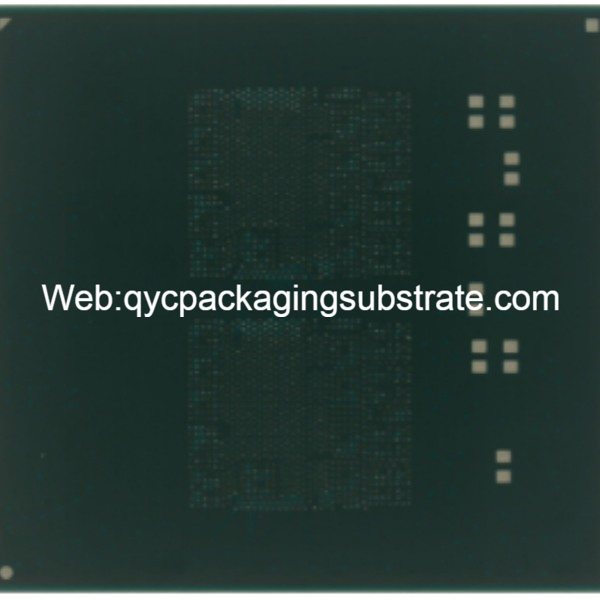
FCBGA Packaging Substrate Vender . We use advanced Msap and Sap technology to build the FCBGA packaging substrates from 4 layer to 20 layers, High quality base materials and fast shipping time. we also do the packaging service.
As an advanced packaging technology, FCBGA packaging substrate (Fine-pitch Ball Grid Array) provides unique advantages for electronic devices by using fine pin arrangements and forming a spherical grid array. In this packaging method, the pins are arranged at a high density, and the spherical grid array formed provides a high degree of reliability and flexibility for the connection of electronic devices.
The fine pin arrangement is one of the distinctive features of the FCBGA package substrate. By arranging the pins more closely, more pins can be accommodated in a limited package space, achieving higher pin density. This allows more functional units to be accommodated within the same package size, improving the performance and functionality of electronic devices.
The formation of spherical grid array is another important feature of FCBGA packaging substrate. Through the spherical grid array, the FCBGA packaging substrate achieves an even distribution of pins, thereby transmitting electrical signals and energy more effectively. This evenly distributed design helps reduce resistance and inductance during signal transmission, improving the signal integrity and stability of electronic devices.
The advantages of FCBGA packaging substrates are not limited to pin density and connection reliability. Thanks to this packaging method, electronic devices are able to dissipate heat more efficiently during operation. The design of the spherical grid array provides a larger heat dissipation surface, which helps accelerate the conduction and dissipation of heat, thereby maintaining the device operating within a stable temperature range.
In general, FCBGA packaging substrate provides electronic devices with multiple advantages such as highly reliable connections, higher pin density, and good heat dissipation performance through its advanced packaging technology. This packaging method is widely used in modern integrated circuit packaging technology, providing strong support for the design and manufacturing of various electronic products.
What is the function of FCBGA packaging substrate?
FCBGA packaging substrates play a variety of important roles in electronic devices and serve as the core component of circuit connections. In addition to providing a reliable electrical connection, it does much more than that. This packaging technology achieves multiple performance advantages through its unique design and structure, making it an indispensable component in the field of modern electronic engineering.
First, the FCBGA package substrate performs well in circuit connections. Its Fine-pitch Ball Grid Array design allows pins to be tightly arranged into a spherical grid array, providing an ideal packaging solution for high-density electronic components. This helps improve the reliability of electrical connections and reduces resistance and inductance during signal transmission, thereby optimizing overall circuit performance.
In addition to electrical connections, FCBGA packaging substrates also have unique advantages in heat dissipation. Its design structure effectively promotes heat dissipation and helps reduce the operating temperature of the circuit. Through the spherical grid array, the FCBGA package substrate provides a larger heat dissipation surface, increasing the contact area with the heat sink, thereby improving heat dissipation efficiency. This is critical in high-performance, high-density electronic devices to prevent performance degradation or damage to circuits due to overheating.
In terms of temperature control, the FCBGA packaging substrate makes it easier for electronic devices to achieve balanced temperature distribution through its unique structural design. This helps prevent certain localized areas from overheating and ensures stable operation of the entire circuit board. By better managing temperature, FCBGA packaging substrates provide electronic devices with longer life and more reliable performance.
Collectively, the FCBGA (Flip-Chip Ball Grid Array) packaging substrate serves not just as a means for circuit connection but as a multifunctional packaging technology. With its meticulously crafted structure, it plays a crucial role in facilitating electrical connections, efficient heat dissipation, and precise temperature control. In the ever-evolving landscape of electronic engineering, the versatile functionality of FCBGA packaging substrates will persistently offer robust support for the development of high-performance, high-density electronic devices.
FCBGA Packaging Substrate
What are the different types of FCBGA packaging substrates?
As a key packaging technology, FCBGA packaging substrate plays a vital role in the electronics industry. Its unique design and structure allow it to be flexibly adapted to different application scenarios and meet diverse needs. The following will introduce in detail the different types of FCBGA packaging substrates and their differences in various aspects.
There are many different types of FCBGA packaging substrates, each of which exhibits excellent performance in specific application scenarios. The following are several common FCBGA package substrate types:
High performance FCBGA
FCBGA packaging substrates designed for high-performance application scenarios usually have higher pin density and more complex internal structures. This makes them excellent at handling large amounts of data, high-speed transmission, and complex computing tasks.
Low power consumption FCBGA
Low-power FCBGA packaging substrate designed for battery-operated equipment and power-sensitive applications. Its optimized power management and heat dissipation design enables it to minimize power consumption while maintaining high performance.
Multi-core FCBGA
FCBGA packaging substrate designed to meet multi-core processing needs. This type of substrate is suitable for applications that need to handle parallel tasks, such as high-performance computing and scientific research.
Each FCBGA package substrate type has unique features and advantages to suit different usage scenarios:
Pin density
High-performance FCBGAs typically have higher pin densities, allowing them to handle more signal and data paths, thereby increasing processing capabilities.
Power consumption control
Low-power FCBGA effectively reduces power consumption by optimizing power management and heat dissipation design, and is suitable for applications that are sensitive to battery life and power consumption.
Parallel processing capability
Multi-core FCBGA achieves more efficient parallel processing by integrating multiple processing cores, and is suitable for applications that need to process multiple tasks simultaneously.
What is the difference between FCBGA packaging substrate and traditional PCB?
Although FCBGA packaging substrate (Fine-pitch Ball Grid Array Packaging Substrate) and traditional PCB (Printed Circuit Board) are both crucial components in electronic devices, there are significant differences in their structures and functions. Let’s dive into the similarities and differences between them, covering everything from PWBs and PCBs, motherboards, substrates to SLP and HDI substrates.
PWBs (Printed Wiring Boards) and PCBs (Printed Circuit Boards) are the core foundation for connecting and supporting electronic components in electronic devices. However, in the FCBGA package substrate, we see a fine pin arrangement and a spherical grid array, which has a slightly different starting point compared with traditional PCB. FCBGA emphasizes higher pin density and more compact layout, providing greater performance potential for electronic devices.
Motherboard: A more advanced connection method
In the field of motherboards, FCBGA packaging substrates adopt more advanced connection methods. Its spherical grid array provides a more stable and reliable electrical connection while enabling a higher level of integration. In comparison, traditional PCBs may use sockets or soldering, and the connection methods are relatively traditional.
Substrate: Differences in structure and heat dissipation
The structure of the FCBGA packaging substrate is more complex and is designed to meet the challenges of high-density layout and complex circuits. At the same time, it has excellent heat dissipation performance and effectively reduces circuit temperature. On the contrary, traditional PCB may be relatively simple in structure, and its heat dissipation performance may not be as superior as FCBGA package substrate.
SLP and HDI substrates: innovative manufacturing technologies
With the development of technology, FCBGA packaging substrates use SLP (Substrate-Like PCB) and HDI (High-Density Interconnect) substrates. These innovative manufacturing technologies provide it with higher performance and reliability. Relatively speaking, traditional PCB may lag behind in innovation in this area.
On the whole, the structural and functional differences between FCBGA packaging substrates and traditional PCBs make the former more suitable for application scenarios with higher performance and space requirements, while the latter may be more suitable for some traditional or low-power electronic equipment. Although they play their own unique roles in the electronics industry, the innovative technology and high-performance characteristics of FCBGA packaging substrates make it an integral part of today’s advanced electronic devices.
What is the main structure of FCBGA packaging substrate? What about manufacturing technology?
Understanding the main structure of the FCBGA packaging substrate is the key to understanding its manufacturing technology. The FCBGA packaging substrate adopts the Fine-pitch Ball Grid Array packaging method, which has precisely arranged pins and forms a spherical grid array. This design is designed to enable high-density, high-performance integration of electronic components.
Substrate material: FCBGA packaging substrates usually use high-performance substrate materials, such as epoxy resin fiberglass (FR-4) or more advanced materials to ensure stability and reliability.
Pin structure: The key part is the pin structure, and its fine arrangement is the basis for achieving high-density connections. These pins connect to the chip via a ball grid array, creating a compact and reliable electrical connection.
Hierarchical structure: The FCBGA packaging substrate adopts a multi-layer design, and the layers are connected through interconnection vias. This hierarchy allows for more electrical signal and power paths, improving the overall performance of the package.
Heat dissipation structure: In order to effectively dissipate heat, the FCBGA package substrate is usually designed with a heat dissipation layer to improve the heat dissipation effect of electronic components. This is critical to keeping circuit temperatures within acceptable limits.
Manufacturing technology of FCBGA packaging substrate
HDI manufacturing technology: High-density interconnect (HDI) technology is an important part of FCBGA packaging substrate manufacturing. This technology enhances circuit board integration by enabling more layers and finer lines on a small-sized substrate.
Improved semi-additive method: The semi-additive method is an innovative technology in FCBGA packaging substrate manufacturing. By adding material to necessary areas rather than the entire substrate, resources can be used more efficiently and manufacturing efficiency can be improved.
Surface treatment technology: The surface treatment of FCBGA package substrate is the key to ensuring reliable connection. Technologies such as metallization and solder paste printing are used to ensure a strong and reliable connection between the pins and the chip.
High-precision process: Manufacturing FCBGA packaging substrates requires highly precise processes, including precise drilling, etching and metallization processes. These steps ensure the accuracy and reliability of every pin and connection.
By understanding the structure and manufacturing technology of FCBGA packaging substrates, we can better understand the key role of this advanced packaging technology in the field of modern electronics. Its highly integrated and advanced manufacturing technology provides a solid foundation for improving the performance of electronic equipment.
What are the characteristics of improved HDI manufacturing technology and semi-additive method?
With the continuous innovation of technology, the manufacturing technology of FCBGA packaging substrate is also undergoing a series of exciting changes. Among them, improved HDI manufacturing technology and new semi-additive manufacturing technology have become the highlights of this technological progress. These two play a key role in improving the performance and reliability of FCBGA packaging substrates.
Improved HDI manufacturing technology
HDI (High-Density Interconnect) manufacturing technology is a technology designed to increase the density of PCB and packaging substrates, bringing significant advantages to FCBGA packaging substrates. Improved HDI technology achieves higher density arrangement of pins and shorter interconnect distances through more precise manufacturing processes. This innovation provides larger wiring space for the FCBGA packaging substrate, helping to increase signal transmission rate and reduce signal transmission delay.
In addition, improved HDI manufacturing technology also optimizes material selection and processing. The use of advanced substrate materials, such as low dielectric constant and low loss materials, helps reduce signal attenuation and improve signal integrity. These improvements work together to make FCBGA packaging substrates perform better in high-frequency applications and large-scale integrated circuits.
New manufacturing technology of semi-additive method
The semi-additive method is a packaging technology that has attracted much attention in recent years. The manufacturing method it adopts is different from the traditional all-additive method, but is more refined and efficient. What’s unique about this technology is that metal is only added to the areas that need to be connected, while remaining non-conductive in other areas. This local addition method reduces manufacturing costs and resource waste, while improving packaging reliability.
The advancement of semi-additive manufacturing technology is reflected in smaller feature sizes and higher manufacturing accuracy. This makes the interconnection structure of the FCBGA package substrate more refined, helping to improve signal integrity and reduce signal crosstalk. In addition, because the manufacturing process of the semi-additive method is more precise, it can also effectively reduce the environmental impact during manufacturing and improve production efficiency.
Performance and reliability improvements
The combination of these two advanced manufacturing technologies has made great progress in the performance and reliability of FCBGA packaging substrates. Improved HDI manufacturing technology provides a more compact and efficient layout and improved electrical performance. The semi-additive rule reduces costs during the manufacturing process, improves reliability, and makes the FCBGA packaging substrate more environmentally friendly.
In essence, the advent of enhanced HDI (High-Density Interconnect) manufacturing technology and semi-additive methods is poised to elevate the prominence of FCBGA (Flip-Chip Ball Grid Array) packaging substrates, particularly in domains such as high-performance computing and communication systems. These technological strides not only play a pivotal role in the production of electronic equipment but also propel the ongoing advancement of the entire industry towards a more sophisticated and efficient trajectory.
Frequently Asked Questions (FAQs)
In this segment, our goal is to address frequently asked questions regarding FCBGA (Flip-Chip Ball Grid Array) packaging substrates, providing insights to assist readers in gaining a comprehensive understanding and application of this advanced packaging technology.
What are the advantages of FCBGA packaging substrate compared with other packaging methods?
Compared with other packaging methods, the FCBGA packaging substrate has a finer pin arrangement and a spherical grid array, providing higher integration and electrical connection reliability. How does this advantage affect the performance and stability of electronic devices?
What is the heat dissipation effect of FCBGA package substrate? How does it compare to other cooling methods?
The FCBGA package substrate provides effective heat dissipation capabilities through its unique design, helping to reduce circuit temperature. We will explore its cooling principles and compare them with traditional cooling methods to evaluate its practical effect in high-performance devices.
What application scenarios are FCBGA packaging substrates suitable for?
Different types of FCBGA packaging substrates are suitable for various application scenarios. We will introduce different types of application fields, including consumer electronics, communication equipment, and industrial control systems, to help readers understand the appropriate scenarios for choosing FCBGA packaging.
What is the development trend of FCBGA packaging substrate manufacturing technology?
As technology continues to evolve, the manufacturing technology of FCBGA packaging substrates is also constantly innovating. We will discuss current trends, including new HDI manufacturing technologies and semi-additive methods, and their impact on FCBGA package substrate performance.
How does the cost of FCBGA package substrate compare to IC packaging?
Cost is a key factor when considering FCBGA packaging substrates. We will compare the cost difference between FCBGA packaging substrate and traditional IC packaging, and explore its advantages in cost-effectiveness.
What is the future development direction of FCBGA packaging substrates?
Understanding the future development direction of FCBGA packaging substrates is crucial for policymakers and engineers. We will study industry trends and explore possible new applications and innovations of FCBGA packaging substrates in future electronic devices.
By answering these frequently asked questions, we hope that readers will have a more comprehensive understanding of the characteristics of FCBGA packaging substrates, so that they can more confidently apply this technology and promote the development of electronic devices.
Summarize
Through an in-depth analysis of the FCBGA packaging substrate, we strive to reveal its importance, versatility and advanced manufacturing technology in electronic devices. FCBGA packaging substrate, as an advanced packaging technology, stands out for its fine pin arrangement and spherical grid array. So, what changes has this technology brought to the performance improvement of electronic devices?
First of all, FCBGA packaging substrate has an importance that cannot be ignored in electronic equipment. By providing a reliable electrical connection, it ensures efficient communication between electronic components, laying a solid foundation for the normal operation of the device. At the same time, its excellent heat dissipation performance reduces the temperature of the circuit and effectively addresses the challenges of heat generation. This enables electronic devices to operate more stably and reliably while providing potential room for improvement in their performance.
Secondly, the FCBGA packaging substrate is not only a medium for electrical connection, it also plays multiple functions. By combating electromagnetic interference (EMI), it further improves the anti-interference ability of electronic equipment and ensures its reliability in complex electromagnetic environments. This provides greater flexibility for use of equipment under different operating conditions.
After having an in-depth understanding of the functions of the FCBGA packaging substrate, we have to pay attention to the advancement of its manufacturing technology. The introduction of improved HDI manufacturing technology and semi-additive method has brought revolutionary changes to the manufacturing of FCBGA packaging substrates. These two advanced technologies not only improve manufacturing efficiency, but also enhance the performance of packaging substrates. Improved HDI manufacturing technology allows more components to be integrated on the substrate, achieving higher integration. The semi-additive law introduces more flexibility into the manufacturing process and provides personalized solutions for different application scenarios.
Taken together, the importance, versatility and advanced manufacturing technology of FCBGA packaging substrates provide solid support for improving the performance of electronic equipment. Through its excellent performance in electrical connection, heat dissipation performance and anti-interference ability, FCBGA packaging substrate has become an indispensable part of modern electronic engineering. With the continuous advancement of manufacturing technology, we have reason to believe that FCBGA packaging substrates will continue to play a key role in future electronic equipment and promote continuous technological innovation.