 Professional Flip-Chip Packaging Substrate Supplier

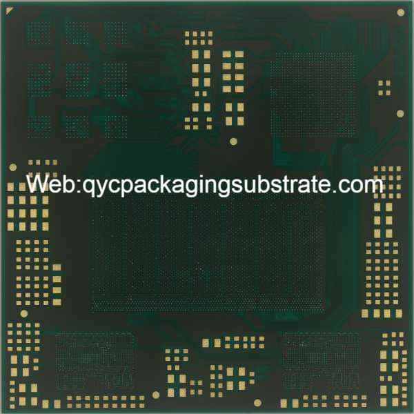
Flip Chip Packaging Substrate Manufacturers and Flip Chip Packaging prototypes up to mid-volume production. High speed material packaging substrate manufacturing. Advanced packaging production process.
Flip Chip Packaging Substrate is an advanced integrated circuit packaging technology that is widely used in the field of microelectronic equipment manufacturing. This technology improves circuit performance and reliability by soldering the chip’s electrical connection side down to the package substrate. The following is a detailed Chinese description of flipping the chip packaging substrate.
Flipping the chip packaging substrate is an innovative integrated circuit packaging technology. Its core idea is to flip the chip so that its electrical connection side faces down and is welded to the packaging substrate. This is different from the traditional chip packaging method, which is to put the electrical connection side of the chip upward and connect it to the packaging substrate through gold wires or other wires. The flipped chip packaging substrate effectively reduces the length and resistance of the electrical connection by directly connecting the bottom of the chip, and improves the speed and performance of signal transmission.
The production process for flip-chip packaging substrates comprises several crucial stages. Initially, the chip undergoes fabrication and testing, followed by soldering onto the packaging substrate through a sequence of procedural steps. In the welding phase, precision technologies like micro-arc welding or laser welding are commonly employed to guarantee a dependable connection between the chip and the substrate. Furthermore, the choice of material for the packaging substrate holds paramount importance. Typically, materials with high thermal conductivity are selected to enhance heat dissipation, ensuring the chip’s stability during operation.
The advantages of flipping the chip packaging substrate are mainly reflected in the following aspects. The first is the improvement of electrical performance. Due to the shortening of electrical connections, resistance is reduced, signal transmission is faster, and energy consumption is reduced. The second is the improvement of heat dissipation performance. The high thermal conductivity of the packaging substrate material allows the chip to better dissipate heat and maintain stability when working under high loads. In addition, flipping the chip package can also achieve a smaller design, making the overall device more compact.
In terms of application, flip chip packaging substrates are widely used in high-performance computers, communication equipment, wireless communication modules and other fields. Especially in some fields that require extremely high electrical performance and heat dissipation performance, such as supercomputers, high-frequency communication equipment, etc., flip chip packaging technology can give full play to its advantages and provide more reliable and efficient solutions.
In general, flipping chip packaging substrates, as an advanced integrated circuit packaging technology, has been widely used in the electronics industry. Its unique design concept and advanced manufacturing process provide reliable support for the performance improvement and size reduction of electronic devices, indicating that it will continue to play an important role in future microelectronics manufacturing.
Flip Chip Packaging Substrate
What are the Materials Used in a Flip Chip Packaging Substrate?
Flip-chip packaging substrate is a key component used in integrated circuit packaging, and its material selection is critical to ensuring the performance and reliability of electronic devices. The main materials used in flip chip packaging substrates will be introduced in detail below.
The fundamental element in flip chip packaging substrates is the substrate material, with organic and inorganic substrates being the common choices. Organic substrates, predominantly fashioned from fiberglass-reinforced epoxy resin (FR-4), offer a lightweight, cost-effective solution suitable for many standard applications. However, in scenarios demanding high performance and high frequency, inorganic substrates take precedence. Typically composed of materials like aluminum nitride (AlN) or aluminum oxide (Al2O3), these inorganic substrates boast exceptional thermal conductivity and electrical insulation properties, rendering them particularly well-suited for applications in flip-chip packaging.
The conductor layer is also a critical component in the manufacturing of flip-chip packaging substrates. The conductor layer usually uses copper because copper has good electrical conductivity properties. The conductor layers are designed to provide electrical connections while also supporting and conducting heat within the structure of the flip chip package.
Another crucial element in packaging is the dielectric material. Positioned atop the conductor layer, it encapsulates the circuit, delivering essential electrical insulation. Widely employed dielectric materials encompass epoxy, polyimide (PI), and fluorinated polymers. Renowned for their commendable electrical insulation properties, mechanical strength, and resistance to high temperatures, these materials collectively ensure the stable operation of circuits across diverse environmental conditions.
In addition to the above main materials, the flip chip packaging substrate may also contain other auxiliary materials, such as solder paste, surface treatment agents, etc., to improve the reliability and durability of soldering.
To sum up, the material selection of flip chip packaging substrate involves many aspects such as substrate, conductor layer and dielectric material. The selection of these materials depends on the specific application scenarios and performance requirements. The purpose is to provide sufficient thermal conductivity, mechanical strength and electrical insulation properties while ensuring circuit functions to ensure that the flip chip package can be used in various complex environments. Works reliably.
What are the types of Flip Chip Packaging Substrate?
Flipping chip packaging substrates is a key technology widely used in electronic device manufacturing, providing an efficient and reliable way to connect and package integrated circuits. Flip chip technology has achieved great success in various applications, providing the possibility for high-performance and miniaturized electronic devices. Here are several common flip chip packaging substrate types:
Organic Substrates
Organic substrate stands out as a prevalent choice for flip chip packaging, typically composed of materials like fiberglass-reinforced epoxy or polyimide. Renowned for their lightweight nature, cost-effectiveness, and ease of fabrication, these substrates find suitability across a spectrum of applications, particularly in low- and medium-power scenarios such as mobile devices and general electronics.
Ceramic Substrates
Ceramic substrates stand out due to their exceptional thermal conductivity and electrical properties, typically crafted from materials like aluminum oxide (alumina) or aluminum nitride (AlN). These substrates find optimal use in high-power and high-frequency applications, particularly in RF and microwave devices. Despite their advantages, it’s worth noting that the production cost of ceramic substrates tends to be relatively elevated.
Silicon Substrates
Silicon substrate is a newer flip chip packaging substrate type that utilizes multi-layer metal connectors on a silicon base. Silicon substrates have excellent thermal conductivity and mechanical properties, making them suitable for high power density applications such as computer servers and communications equipment.
Glass Substrates
Glass substrates excel in some specific applications, particularly where superior packaging transparency or biocompatibility is required. Glass substrates can realize complex circuit structures through microelectronics processing technology and are suitable for some biosensors and medical equipment.
Multilayer Substrates
Multilayer film substrate is a composite substrate formed by stacking multiple layers of films together, providing more wiring layers and higher integration. This type of substrate is often used in high-density integrated circuits to enable more complex circuit connections.
Sapphire Substrates
Sapphire substrates are favored for their excellent performance in high-temperature and high-frequency applications. They provide good thermal stability and electrical performance for some special applications, such as LED chip packaging.
Overall, selecting the appropriate flip chip packaging substrate type depends on the requirements of the specific application, including considerations such as power consumption, frequency, thermal management, and manufacturing cost. Various types of substrates play key roles in different fields, providing diverse and efficient packaging solutions for electronic devices.
When is It Ideal to Use Flip Chip Packaging Substrate?
Flip Chip Packaging Substrate is an advanced packaging technology that has many advantages and is particularly suitable for specific electronic devices and application scenarios. Here are some ideal scenarios when using flipped chip packaging substrates:
Flipping chip packaging substrates demonstrate superior performance in the realm of high-density integrated circuit designs. Their distinctive design allows for a more efficient reduction in package size and enhanced component integration. This makes them particularly well-suited for compact electronic devices like smartphones, wearables, and other miniature electronics. Beyond simply achieving smaller dimensions, this technology facilitates lighter designs, aligning seamlessly with the contemporary demand for thin, light, short, and small (SLIM) requirements in modern electronic devices.
Furthermore, flip chip packaging substrates shine in high-performance and high-frequency applications. The direct connection of the chip to the substrate in flip chip packages results in a shortened length of connecting wires, minimizing signal transmission delays. This attribute is critical in applications requiring high-speed data transmission and precise timing, such as communication equipment, radar systems, and other high-frequency electronics. Additionally, the flip chip packaging configuration contributes to improved signal integrity and reduced signal distortion by mitigating the inductance of connecting wires, rendering it an ideal choice for high-frequency electronic devices.
Third, flipping the chip packaging substrate provides excellent thermal management. Its design directly connects the chip to the heat dissipation substrate, effectively improving heat conduction efficiency. This is critical for applications requiring high power density and superior thermal performance, such as computer servers, power amplifiers and other high-power electronic equipment. By transferring heat to the thermal substrate more efficiently, flipping the chip package helps prevent the chip from overheating and improves device reliability and stability.
In addition, the flip chip packaging substrate also performs well in flip-chip soldering processes (C4, BGA, etc.), helping to improve production efficiency and reduce manufacturing costs. Its flip-chip welding process characteristics enable the production line to complete the welding process more efficiently, improving production speed and packaging quality.
Overall, the advantages of flipped chip packaging substrates in terms of miniaturization, high performance, high frequency, and thermal management make them ideal for many modern electronic applications. However, the specific choice of whether to use a flipped chip packaging substrate must also consider factors such as the specific needs of the product, budget, and production process.
How is a Flip Chip Packaging Substrate Manufactured?
Flip chip packaging substrate is an advanced electronic packaging technology that plays a key role in modern electronic devices. Manufacturing such substrates involves multiple complex steps, and the manufacturing process of flip-chip packaging substrates is described in detail below.
Subsequently, the second step encompasses the meticulous surface preparation of the substrate. This entails a thorough cleaning process and the application of an adhesive layer to guarantee a secure attachment of the chip in subsequent stages. Specialized solvents and cleaning agents are often employed during the cleaning process to eliminate impurities and contaminants from the surface.
Moving forward, the manufacturing process proceeds with the masking step. Here, advanced photolithography technology comes into play, coating the substrate’s surface with a photosensitizer. The surface is then exposed to ultraviolet light, forming the desired pattern. This pattern serves as the blueprint, defining the structure and connection points of the circuit.
After pattern formation, etching and deposition steps are performed. This involves using chemical corrosives to remove unwanted parts of metal while depositing metal in needed areas to form circuits and connections. These steps often involve multiple iterations to build complex circuit structures.
Next is the installation of the flip chip. This involves turning the chip over so that its electrical connections face down and connecting it to a metallized area of the substrate via soldering or other connection techniques. This ensures a shorter signal path, improving the performance of the circuit.
After completing the chip installation, perform insulation and protection processing. This involves applying an insulating layer to prevent shorts between circuits and protect the chip from the external environment. The selection and application of insulation is an important step in ensuring equipment reliability and stability.
Finally, final testing and inspection takes place. Functional verification and quality inspection of manufactured flip chip packaging substrates is performed using various test equipment and techniques to ensure that they comply with design specifications and standards.
Overall, the manufacturing process of flip-chip packaging substrates is a complex and sophisticated process that requires a high degree of process control and technical expertise. This packaging technology is increasingly used in modern electronic equipment, providing reliable solutions for high-performance and miniaturized electronic products.
Where to Find Flip Chip Packaging Substrate?
Flip Chip Packaging Substrate is a key material used in integrated circuit packaging and plays an important role in modern electronic devices. Finding Flip Chip Packaging Substrate involves many aspects, including supplier networks, market research and technology evaluation.
First, suppliers of Flip Chip Packaging Substrate can usually be directly searched through the Internet at our website. On our website, we have many electronic materials and packaging materials, and we can provide various types of substrates, including substrates suitable for Flip Chip packaging. Secondly, you can learn about Flip Chip Packaging Substrate by attending relevant electronics exhibitions and industry conferences. These exhibitions and conferences are often important platforms for the electronics industry to communicate and showcase new technologies. On these occasions, you can directly learn more about their product features, performance and customization options.
In addition, professional electronic materials and packaging materials market reports are also useful resources to understand Flip Chip Packaging Substrate. These market reports are usually prepared by professional research organizations and provide detailed information on industry trends, market shares, and key players. By analyzing market reports, you can understand the current market trends of Flip Chip Packaging Substrate on the market and conduct a preliminary evaluation of its products.
When choosing Flip Chip Packaging Substrate, you must consider not only its product quality and performance, but also its delivery capabilities, technical support, and after-sales service. The products and manufacturing processes produced by our company are very lean, and the quality of the products produced by our company can be absolutely guaranteed.
In general, the process of finding Flip Chip Packaging Substrate requires a comprehensive consideration of multiple factors, including online searches, participation in exhibitions and conferences, analysis of market reports, and comprehensive consideration of the supplier’s credibility and experience. Through these channels, you can find high-quality Flip Chip Packaging Substrate that meets your specific needs and learn about us on multiple levels.