 Professional Flip-Chip Packaging Substrate Supplier

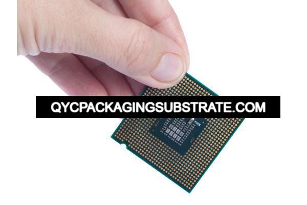
Glass Materials Package Substrates Manufacturer. we can produce the best samllest bump pitch with 100um, the best smallest trace are 9um.
In today’s electronics industry, Glass Materials Package Substrates play a crucial role. As one of the core components of modern electronic equipment, they are not only the basis for supporting key components such as circuits and chips, but also provide solid support for the functions and performance of various devices. Whether it is consumer electronics, communication equipment or automotive electronics, glass material packaging substrates bear important responsibilities and promote the continuous development of electronic technology.
What are Glass Materials Package Substrates?
Glass material packaging substrate is a vital component of electronic equipment, playing a key role in connecting and supporting circuits and chips. They usually consist of a glass substrate and a conductive layer and are widely used in modern electronics.
First, as the main body of the packaging substrate, the glass substrate has excellent physical properties and chemical stability. Compared with traditional substrate materials, such as plastics or ceramics, glass substrates have higher thermal conductivity and dimensional stability, and can maintain stable performance in extreme temperature environments. This stability enables the glass material packaging substrate to work reliably under harsh conditions such as high temperature and high pressure, making it suitable for various industrial and commercial applications.
Secondly, the conductive layer is a key component of the glass material packaging substrate and is used to connect circuits and chips. The conductive layer is usually composed of a metal film or other conductive materials, and is formed on the glass substrate through printing, etching and other processes. These conductive layers provide channels for electronic signal transmission, allowing various components on the circuit board to be connected to each other to achieve the normal operation of electronic equipment.
Glass Materials Package Substrates Manufacturer
Overall, glass material packaging substrates play an integral role in electronic devices. They provide stable support and connections for circuits and chips, ensuring device performance and reliability. With the continuous development of electronic technology, glass material packaging substrates will continue to play an important role in promoting the progress and innovation of electronic equipment.
Glass Materials Package Substrates design Reference Guide.
In the design process of modern electronic devices, glass material packaging substrates play a vital role. Its design quality directly affects the performance and reliability of the equipment. Therefore, when designing a glass material packaging substrate, multiple factors need to be considered to ensure that it meets the needs of the device and has good performance and reliability.
Circuit layout
Good circuit layout is key to designing high-performance packaging substrates. During the design process, ensure that the circuit layout is compact and reasonable to avoid signal interference and electromagnetic interference. Reasonable layout can minimize signal transmission paths and improve the stability and reliability of the circuit.
Material selection
Choosing the right material is critical to the performance of glass material packaging substrates. The selection of glass substrate should consider factors such as its thermal expansion coefficient, mechanical strength and chemical stability. The materials of the conductive layer and the insulating layer also need to be selected according to actual needs to ensure the stability and reliability of the circuit.
Packaging technology
Packaging technology directly affects the performance and reliability of glass material packaging substrates. Factors such as cost, production efficiency and performance requirements should be taken into consideration when selecting a packaging technology. Common packaging technologies include patch packaging, ball grid array (BGA) packaging, etc. Each technology has its applicable scenarios, advantages and disadvantages.
Design Guidelines provide advice and guidance
Design Guidelines provide critical advice and guidance on the design of glass packaging substrates. These suggestions cover circuit layout optimization, material selection, packaging technology application, etc. By following the recommendations of the Design Guide, you can maximize the performance and reliability of glass material packaging substrates while reducing design and production costs.
Designing glass material packaging substrates requires considering multiple factors and following the recommendations and guidance provided by the design guide. Only by fully considering circuit layout, material selection, packaging technology and other factors during the design process can we design a glass material packaging substrate with excellent performance, reliability and stability, and provide solid support for the development of electronic equipment.
This article details the factors to consider when designing glass packaging substrates and highlights the importance of design guidelines. By following the suggestions and guidance provided by the design guide, a packaging substrate with excellent performance, reliability and stability can be designed to provide solid support for the development of electronic equipment.
What material is used in Glass Materials Package Substrates?
The material composition of glass material packaging substrates is crucial, as they directly affect the performance and reliability of the substrates. Typically, glass material packaging substrates are composed of specific types of glass, conductive metals, and insulating materials.
First of all, glass is one of the basic components of glass material packaging substrates. This glass usually has a high degree of flatness and uniformity to ensure the stability and reliability of the circuit board. In addition, it has good optical transparency and chemical stability, making it an ideal choice for many high-end electronic devices.
Secondly, the conductive metal layer is one of the key components of the glass material packaging substrate. These metal layers are usually made of materials such as copper or aluminum and have excellent electrical and thermal conductivity. They are precisely deposited on the surface of the glass substrate to form channels for circuit connection and signal transmission, providing support for the normal operation of electronic equipment.
In addition, insulating materials also play a vital role in glass material packaging substrates. These materials are often used to cover and protect conductive metal layers to prevent short circuits and other circuit failures. Common insulating materials include epoxy resin and polytetrafluoroethylene (PTFE), which have good insulation and high temperature resistance and can effectively protect the stability and safety of circuit boards.
In general, the glass, conductive metal and insulating materials used in glass material packaging substrates have good conductivity, insulation and high temperature resistance, and are suitable for various electronic application scenarios. Their precise combination and excellent performance provide a solid foundation for the development of modern electronic equipment and promote the continuous innovation and progress of the electronics industry.
What size are Glass Materials Package Substrates?
Glass material packaging substrates play a key role in electronic devices, and their sizes vary according to different application scenarios and equipment requirements. From microdevices to large industrial equipment, glass material packaging substrates come in a wide range of variability to meet a variety of needs.
For miniature devices, such as smartphones, tablets, and wearables, glass material packaging substrates often need to be very small in size. This minimizes the size and weight of the device while ensuring its performance and functionality are not compromised. In these small devices, the size of the glass packaging substrate may be only a few square centimeters or even smaller.
For large industrial equipment, such as communication base stations, industrial control systems and medical equipment, the size of the glass material packaging substrate may be relatively large. These devices typically require more circuit support and connections, so the size of the substrate can reach tens of square centimeters or more.
In addition to the size, the glass material packaging substrate also needs to consider its thickness. In some applications, especially mobile devices that require thin and light designs, thin glass material packaging substrates are particularly important. In some industrial and automotive applications, thicker substrates may be better suited to withstand the challenges of high-temperature and high-pressure environments.
Overall, glass material packaging substrates are available in a wide range of sizes and can be customized to suit the size and performance requirements of different devices. This flexibility makes glass material packaging substrates ideal for a variety of electronic devices, providing stable and reliable circuit support and connections, whether in micro devices or large industrial equipment.
The Manufacturer Process of Glass Materials Package Substrates.
The manufacturing process of glass material packaging substrates is a complex and precise process, which involves multiple key steps. Each step requires precise operation and strict control to ensure that the quality and performance of the final product meet the requirements.
First of all, the first step in manufacturing a glass material packaging substrate is design. During the design phase, engineers need to determine the size, layout, and hierarchy of the substrate based on the product’s needs and specifications. This process needs to take into account factors such as circuit connections, signal transmission, and thermal management to ensure that the final design can meet the product’s functional and performance requirements.
Next comes the printing stage. At this stage, the designed circuit diagram is transferred to the substrate, usually using printing technology to print conductive materials (such as copper) on the glass substrate to form circuit lines. This step requires precision printing equipment and technology to ensure the accuracy and reliability of the circuit.
Then comes etching. Etching is the process of removing unwanted parts from a conductive layer to form the shape and connections of a circuit. Chemical etching techniques are usually used to remove the conductive material, leaving only the designed circuit traces. This step requires strict control of the concentration and temperature of the chemical solution to ensure the accuracy and consistency of etching.
Finally comes assembly. At this stage, the electronic components are mounted onto the substrate, often using soldering techniques to connect them to the circuit. This process involves precision assembly equipment and techniques to ensure the correct placement of components and quality of connections.
In general, manufacturing glass material packaging substrates is a process that requires precision equipment and a high level of technology. Each step requires strict control and monitoring to ensure the quality and performance of the final product meets requirements. The exquisiteness and perfection of these processes have made glass material packaging substrates one of the first choices for many electronic devices.
The Application area of Glass Materials Package Substrates.
As an important part of the electronics industry, glass material packaging substrates play a key role in various fields. They not only provide stable circuit support and connections, but also provide basic support for the functionality and performance of various products. The following are the applications of glass material packaging substrates in consumer electronics, communications, automobiles, medical and other fields:
Consumer Electronics
In the field of consumer electronics, such as smartphones, tablets, smart home devices, etc., glass material packaging substrates are widely used. They play an important role in connecting various chips and circuits in these devices, ensuring the stability and performance of the device.
Communication
In the field of communications, such as base station equipment, routers, optical fiber communication equipment, etc., glass material packaging substrates also play an important role. They provide reliable circuit support to ensure efficient operation and stable connections of communication equipment.
Car
In the field of automotive electronics, glass material packaging substrates are widely used in automotive electronic control units (ECUs), in-car entertainment systems, navigation systems, etc. They can withstand high temperatures, vibrations and other harsh environments, ensuring the reliability and stability of automotive electronic systems.
Medical
In the field of medical devices, such as medical imaging equipment, pacemakers, life monitoring instruments, etc., glass material packaging substrates also play a key role. They have excellent chemical stability and biocompatibility, making them suitable for use in medical environments and ensuring device accuracy and reliability.
To sum up, glass material packaging substrates play an important role in consumer electronics, communications, automobiles, medical and other fields, providing reliable support for the performance and stability of various products. With the continuous development of technology, the application scope of glass material packaging substrates will be further expanded, injecting new impetus into the development of the electronics industry.
What are the advantages of Glass Materials Package Substrates?
Glass material packaging substrates are very popular in the field of electronic manufacturing. One of its advantages is its excellent thermal conductivity. Thermal conductivity refers to the ability of a material to transfer heat, and glass substrates can conduct heat efficiently, helping to effectively disperse heat in electronic devices to maintain stable performance of the device. Especially for high-power electronic equipment, good thermal conductivity can effectively reduce the temperature of the equipment and extend its service life.
In addition, the glass material packaging substrate also has excellent chemical stability. Glass materials are not susceptible to chemical attack, have high corrosion resistance, and can maintain stable performance under harsh environmental conditions. This enables glass material packaging substrates to maintain reliability in various application scenarios, whether it is high temperature environments in industrial control systems or humid environments in medical equipment.
In addition, dimensional stability is another advantage of glass material packaging substrates. Glass materials have a low thermal expansion coefficient, which means that their dimensions change less when the temperature changes. This dimensional stability makes glass substrates excellent in high-precision applications such as precision instruments, optical equipment, etc. In these fields, glass material packaging substrates can ensure the stable position and connection of electronic components and ensure the performance and accuracy of the equipment.
To sum up, glass material packaging substrates have become the preferred material for many electronic devices due to their excellent thermal conductivity, chemical stability and dimensional stability. Its wide application in the field of electronic manufacturing benefits from these advantages, providing reliable support for the stable operation and performance improvement of various types of equipment.
FAQ
What is the difference between glass material packaging substrate and traditional packaging substrate?
Traditional packaging substrates usually use organic substrates (such as FR-4) as the base material, while glass material packaging substrates use glass substrates, which have higher thermal conductivity and chemical stability. Glass substrates can also provide better dimensional stability and bending resistance, making them suitable for applications requiring higher stability.
How long is the production cycle for glass material packaging substrates?
The production cycle of glass material packaging substrates usually depends on the specific design requirements and production processes. Generally, it takes several weeks to several months from design to final delivery. Complex designs and high precision requirements may take longer to complete.
What is the cost of glass material packaging substrate?
The cost of glass material packaging substrates depends on multiple factors, including substrate material, size, number of layers, production process, etc. The cost of glass material packaging substrates may be slightly higher compared to traditional packaging substrates, but considering its excellent performance and stability, this additional cost is worth the investment.
How environmentally friendly are glass material packaging substrates?
Glass material packaging substrates usually have better environmental performance because the glass substrate is an inorganic material and does not contain organic solvents and toxic substances. In addition, the high-temperature melting and reuse properties of glass materials also help reduce waste generation, in line with the requirements of modern environmental awareness.