 Professional Flip-Chip Packaging Substrate Supplier

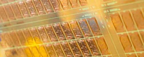
Glass Substrates manufacturer. Advanced glass packaging substrate manufacturer, advanced production equipment and team, we produce high layer glass substrate and ABF substrate from 2 layer to 22 layers.
In modern electronic products, printed circuit boards (PCBs) are an indispensable component. However, for manufacturing PCBs, do we often consider using glass substrates? This article will take an in-depth look at the applications and advantages of glass substrates in PCB manufacturing, as well as its importance in the modern electronics industry.
What is a glass substrate?
Glass substrates play a vital role in modern electronics manufacturing. As a common base material, it provides a stable and reliable foundation for the manufacturing of printed circuit boards (PCBs). So, what is a glass substrate and why is it so popular?
Glass substrate is a basic material with glass as the main component. Common materials include glass fiber, borosilicate glass, etc. Compared with other substrate materials, glass substrate has excellent flatness and surface finish, which makes it one of the ideal choices for PCB manufacturing.
First, the flatness of the glass substrate is critical to PCB design and manufacturing. Due to the high flatness of the glass substrate surface, it ensures precise mounting and connection of electronic components during the PCB manufacturing process. This flatness ensures the stability of circuit layout and components on the PCB, thereby improving the overall performance and reliability of electronic products.
Secondly, the glass substrate has good chemical stability, which gives it a unique advantage in PCB manufacturing. Glass substrates are less susceptible to chemical corrosion and environmental changes, thus maintaining PCB stability and durability. This chemical stability means that PCB can work in various harsh environments, such as high temperature, high humidity and chemical corrosion, and still maintain good performance.
In addition, the surface finish of the glass substrate also facilitates PCB manufacturing. Due to its smooth surface, glass substrates ensure precision and consistency in the PCB manufacturing process. This surface finish helps ensure precise layout of circuits and accurate mounting of components on the PCB, thereby increasing PCB production efficiency and quality.
In general, glass substrate, as a high-quality basic material, plays an important role in PCB manufacturing. Its good flatness, chemical stability and surface finish make it one of the ideal choices for PCB manufacturing. Therefore, glass substrates have become an integral part of modern electronic manufacturing.
Glass Substrates Manufacturer
How to design a PCB using glass substrate?
Designing a PCB using a glass substrate involves a series of critical steps, from component layout to circuit design, all of which need to take into account the characteristics and limitations of the glass substrate. First, designers need to consider the flatness and dimensional stability of the glass substrate. Glass substrates usually have high flatness, which is crucial for achieving high-density component layout. During the component layout stage, designers need to arrange electronic components reasonably to ensure that they can be arranged closely without affecting the electrical connections between each other.
Secondly, designers need to consider the thermal conductivity of the glass substrate. Since glass substrates have relatively poor thermal conductivity, heat dissipation measures need to be considered in the design to ensure that electronic components do not overheat. This may involve adding thermal vias to the PCB design or using accessories such as heat sinks.
Additionally, designers need to consider the mechanical strength and brittleness of the glass substrate. Glass substrates may be more susceptible to mechanical stress than other substrate materials, so it is necessary to strengthen the support structure or reduce the mechanical stress on the substrate in the design.
In the circuit design stage, designers need to optimize the signal transmission path based on the dielectric constant and loss factor of the glass substrate. This includes considering signal trace routing, width, and spacing to minimize signal attenuation and crosstalk.
Finally, after the design is completed, designers need to conduct rigorous design verification and simulation analysis to ensure that the PCB design meets the expected performance indicators and reliability requirements. This may involve using electromagnetic field simulation software to model performance in areas such as signal integrity and electromagnetic compatibility.
In short, designing a PCB using a glass substrate requires comprehensive consideration of its characteristics and limitations. From component layout to circuit design, the characteristics of the glass substrate need to be fully considered during the design process, and corresponding measures must be taken to optimize the design and ensure the final PCB design. Able to meet performance and reliability requirements.
What is the glass substrate processing process in PCB manufacturing?
In PCB manufacturing, the processing process of glass substrate is a key link, which directly affects the quality and performance of the final PCB. The following will introduce in detail the processing process of glass substrates in PCB manufacturing:
The first step in PCB manufacturing is to prepare the substrate. As a common substrate material, glass substrate requires strict preparation. This includes cleaning and treating the glass surface to ensure its flatness and surface quality.
The next step is to form a copper layer on the surface of the glass substrate to form circuit connections. This is usually achieved through chemical methods or physical plating. The uniformity and thickness of the copper layer are critical to the reliability of the circuit connection.
Forming the required circuit pattern on the copper layer is one of the key steps in PCB manufacturing. This is usually accomplished by photolithography and etching, so that only the conductive parts remain on the substrate to form the circuit connections.
Hole drilling is an important channel for assembling components on PCB, so drilling holes on glass substrates is also a necessary step in the manufacturing process. These holes will be used to solder components and make circuit connections.
Finally, the glass substrate is surface treated to protect the copper layer and circuit connections from the environment. This includes applying protective coatings such as solder paste and solder mask, as well as surface finishing.
Each step requires precise control and strict execution to ensure the quality and performance of the PCB reaches the expected level. From substrate preparation to final surface treatment, each step plays a vital role, affecting the functionality and reliability of the PCB. Therefore, in the PCB manufacturing process, careful management and control of the glass substrate processing process is crucial.
What is the cost of manufacturing PCB with glass substrate?
The cost of manufacturing PCBs using glass substrates shows diverse characteristics under the influence of many factors. Compared with other substrate materials, the cost of glass substrates is affected by factors such as material cost, processing complexity, and manufacturing volume.
First, the material cost of glass substrates is usually relatively low. Glass is a common basic material. Compared with some high-performance special materials, such as ceramic substrates or flexible substrates, the cost of glass is more affordable. This makes choosing glass substrate as one of the PCB materials an economical and reasonable choice.
Secondly, processing complexity is also one of the important factors affecting the manufacturing cost of glass substrates. Because glass substrates are relatively fragile, more delicate handling and control are required during processing. Especially in the manufacturing process of multi-layer PCB, more precise processes are required to ensure the connection and insulation between the layers. These additional process steps and technical requirements may increase manufacturing costs.
Finally, manufacturing volume is also one of the key factors affecting the cost of glass substrate manufacturing. Generally speaking, as manufacturing volume increases, unit prices decrease because manufacturers can use production equipment and resources more efficiently. PCBs produced in small batches usually have a higher cost, while mass production is relatively cheaper.
In summary, the cost of manufacturing PCBs with glass substrates is comprehensively affected by multiple factors such as material cost, processing complexity, and manufacturing volume. When selecting PCB materials, these factors need to be considered comprehensively and decisions made based on specific project needs.
What are the commonly used glass substrate materials in PCB manufacturing?
In PCB manufacturing, common glass substrate materials include glass fiber reinforced epoxy resin (FR-4), glass fiber reinforced polyimide (PI), and glass fiber reinforced polyamide (PA).
First, let us understand the characteristics of these commonly used materials:
Fiberglass Reinforced Epoxy (FR-4): FR-4 is one of the most common glass substrate materials used in PCB manufacturing. It has excellent mechanical properties and high temperature resistance and is suitable for most application scenarios. FR-4 substrate has high electrical insulation properties and good chemical stability, and can meet the requirements of most electronic products.
Glass fiber reinforced polyimide (PI): PI substrate has excellent high temperature stability and mechanical properties and is a high-performance substrate material. Its main advantages include good heat resistance, chemical stability and electrical insulation properties, making it suitable for applications in high temperature environments and special industrial fields.
Glass fiber reinforced polyamide (PA): PA substrate has good mechanical and thermal properties and performs well in high temperature environments. Its advantages include high strength, low water absorption and excellent electrical insulation properties, making it suitable for some applications that require high mechanical properties and stability.
Understanding the characteristics of these different materials can help in selecting the appropriate glass substrate for a specific application. For example, for some applications that require high temperature resistance, PI or PA substrates can be selected; while for general electronic product manufacturing, FR-4 substrates may be a more economical choice. At the same time, factors such as cost, processing performance, and application environment must also be taken into consideration to comprehensively evaluate and select the most appropriate glass substrate material.
In summary, different glass substrate materials have their own advantages and disadvantages, and choosing the appropriate material depends on specific application needs and manufacturing requirements. By deeply understanding the characteristics of these materials, we can better provide technical support and solutions for PCB manufacturing.
Who is producing PCBs using glass substrates?
When it comes to producing PCBs using glass substrates, there are many manufacturers involved, including some leading electronics manufacturing companies and professional PCB manufacturers. In this area, the company is a trusted industry leader.
Our company has advanced production equipment and rich experience and is committed to providing high-quality PCB solutions, including PCBs manufactured using glass substrates. Through continuous technological innovation and quality control, the company has established a good reputation and become a trusted partner of customers.
As a professional PCB manufacturer, our company can not only meet customers’ customized needs, but also provide a full range of technical support and services. From initial design to final delivery, our team will work closely with clients to ensure each project is delivered on time and to the highest standards.
In addition to high-quality products and excellent services, our company also pays attention to environmental protection and sustainable development. We take a range of measures to reduce our environmental impact, including using environmentally friendly production processes and materials, and implementing waste recycling and reuse programs.
By cooperating with our company, customers can confidently choose PCBs made with glass substrates, obtain high-quality, reliable products, and enjoy professional technical support and excellent customer service.
In the field of PCB manufacturing, choosing our company is a wise decision. We will wholeheartedly provide you with satisfactory solutions and promote the success of your project.
What are the 5 traits of good customer service?
Good customer service is one of the key factors in the success of any business. It is not just about simply meeting customer needs, but also an important means of establishing long-term relationships and promoting word-of-mouth communication. Here are five qualities of good customer service:
Prompt response: Customers expect prompt feedback when they encounter problems or ask questions. Timely responses demonstrate attention to customer needs and sensitivity to problem solving. By responding promptly, customer dissatisfaction and misunderstanding can be effectively avoided and trust and reliability built.
Expertise: Good customer service requires extensive expertise to provide accurate, reliable solutions. Understanding the details of a product or service and being able to explain it clearly to customers will not only satisfy customers’ needs, but also enhance customers’ trust and loyalty to the brand.
Empathy: Understanding and empathizing with customers’ emotions and needs is an important trait in providing excellent customer service. By expressing empathy and making customers feel understood and cared for, you can build positive customer relationships and promote customer satisfaction and loyalty.
Adaptability: Different customers have different needs and preferences, and good customer service requires flexibility and adaptability, being able to adjust and customize according to the customer’s specific situation and requirements. Through flexible service methods and personalized solutions, we can meet the diverse needs of customers and improve customer experience and satisfaction.
Effective communication: Clear and accurate communication is the foundation of good customer service. Through effective communication, information misunderstandings and communication barriers can be avoided, ensuring that customers have a clear understanding and expectations of the service process and results. At the same time, active communication can also enhance trust and cooperation between customers and enterprises.
To sum up, prompt response, expertise, empathy, adaptability and effective communication are the key attributes that build good customer service. By continuously improving these characteristics, companies can establish good customer relationships and increase competitiveness and market share.
Frequently Asked Questions
What are the advantages of glass substrates over other substrate materials?
Glass substrates have unique advantages over other common substrate materials, such as FR-4 (fiberglass reinforced epoxy resin), metal substrates, etc. First, the glass substrate has excellent flatness, which makes it suitable for high-density circuit designs and can accommodate more lines and components, thereby improving the performance of the circuit board. Secondly, the glass substrate has excellent chemical stability and can maintain stable electrical properties under various environmental conditions, thereby enhancing the reliability and durability of the circuit board. In addition, the glass substrate also has good heat resistance and can remain stable in high temperature environments, making it suitable for some special application fields, such as automotive electronics, aerospace, etc.
How long is the processing cycle for manufacturing PCB using glass substrate?
The processing cycle of glass substrate manufacturing PCB varies depending on the manufacturing complexity and mass production scale. Generally speaking, the PCB processing cycle for small batch production may be around a few days to a week, while the PCB for mass production may take longer, which may extend to several weeks or even longer. In addition to the manufacturer’s production capacity, the processing cycle is also affected by factors such as design document preparation, process settings, and material supply. Therefore, when selecting a manufacturer, a balance between the project’s time requirements and production capabilities needs to be considered.
Are there environmentally friendly glass substrate options for PCB manufacturing?
Yes, with the increasing awareness of environmental protection, more and more PCB manufacturers are beginning to pay attention to environmental issues and provide environmentally friendly glass substrate options. These environmentally friendly options often include using lead-free solder, adopting low-pollution chemical processing methods, and implementing scrap recycling and reuse programs. Through these environmental protection measures, not only can the impact of the PCB manufacturing process on the environment be reduced, but the sustainability of the circuit board can also be improved, in line with the needs of modern society for sustainable development.
What are the advantages of glass substrates over other substrate materials?
Glass substrates offer several outstanding advantages. First, they have excellent flatness, which means that during the PCB manufacturing process, higher precision and denser wiring can be achieved, making the board more stable and reliable. Secondly, the glass substrate has high chemical stability and can resist the erosion of various chemicals, so it is widely used in special environments. In addition, glass substrates have good thermal conductivity and help dissipate heat, which is crucial for high-power electronic devices. Overall, glass substrates excel in PCB designs for high performance and special applications.
How long is the processing cycle for manufacturing PCB using glass substrate?
The processing cycle time for PCB manufacturing varies based on a variety of factors, including design complexity, manufacturing volume, and manufacturer’s production capabilities. Generally speaking, the processing cycle for PCBs manufactured using glass substrates usually ranges from a few days to a few weeks. For low-volume production or prototype manufacturing, the machining cycle may be shorter, while large-scale production may take longer to complete. It is recommended to communicate with the manufacturer before starting manufacturing to determine the accurate processing cycle time.