 Professional Flip-Chip Packaging Substrate Supplier

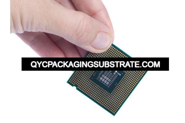
What is High Frequency Package Substrate?
High frequency package substrate manufacturer. the Package Substrate will be made with Rogers series materials and other same grade high frequency base materials. or other high speed materials. such as: Showa Denko and Ajinomoto High speed materials.
Its compelling signal transmission performance makes it a focus of today’s electronic device design. So, what is unique about High Frequency Package Substrate in this field?
In the definition of high-frequency Package Substrate, we must first understand the “high-frequency environment”. This means that this kind of circuit board mainly deals with scenarios that require higher frequency data transmission and precise signal processing.
This circuit board uses advanced technology and materials to ensure excellent performance in high-frequency environments. This may include microfabrication, high-density wiring and other processes to meet the high requirements for signal transmission stability and accuracy.
Secondly, high-frequency Package Substrate has broad applicability in different types of applications. Whether it is 5G communication equipment, satellite communication systems, or radio frequency modules, High Frequency Package Substrate can provide excellent solutions. Its flexibility and efficiency make it ideal for a variety of high-frequency equipment.
The distinctive design and high-performance capabilities of the High Frequency Package Substrate set it apart in the realm of electronic engineering. In the context of ever-growing complexity and heightened performance requirements in electronic devices, it transcends being merely a circuit board. Instead, it serves as a pivotal component that catalyzes scientific and technological advancements.
What are the types of high-frequency Package Substrate?
In the realm of electronic engineering, high-frequency package substrates play a pivotal role as a diverse range of circuit board types, among which the Ball Grid Array (BGA) stands out prominently. Characterized by a configuration of solder balls arranged spherically with spaced intervals, BGA serves as a crucial high-frequency package substrate, establishing connections with the motherboard. This design not only ensures elevated connection density but also enhances heat dissipation performance. Consequently, BGA finds its application in scenarios demanding stringent requirements for high-speed data transmission and efficient thermal management, such as 5G communication equipment and high-performance computing modules. It represents a sophisticated solution tailored to meet the unique demands of these specific application scenarios.
The design of CSP is committed to minimizing the package size, reducing the package size to be similar to the chip itself. This compact design is suitable for devices that require small size and light weight, such as portable communications equipment and drone control units. CSP achieves a smaller package while maintaining high performance, helping to improve the overall integration of the device.
Different types of high-frequency Package Substrate play key roles in specific application scenarios based on their structure and design. BGA is often used in devices that need to process large amounts of data and generate high heat, while CSP is more suitable for applications that focus on lightweight and small design. This differentiated design allows engineers to choose the most appropriate high-frequency Package Substrate type based on the specific needs of the project to achieve the best performance and reliability.
Overall, the diversity of high-frequency Package Substrate provides greater flexibility and choice for electronic engineering. By in-depth understanding of the characteristics and application scenarios of each type, engineers can more accurately select the high-frequency Package Substrate suitable for their projects, injecting more powerful performance and innovation into future electronic devices.
High frequency package substrate
What are the advantages of high-frequency Package Substrate?
The advantage of high-frequency package substrate lies in its significant superiority over traditional circuit boards in terms of integration, signal transmission performance, and heat dissipation performance. Below is a closer look at these benefits.
First of all, high-frequency Package Substrate performs well in terms of integration. Due to the use of advanced packaging technology, high-frequency Package Substrate enables more compact and lighter designs. This allows electronic devices to accommodate more components and functions in a limited space, thereby improving overall integration.
Secondly, high-frequency Package Substrate performs outstandingly in signal transmission performance. In high-frequency environments, the stability of signal transmission is crucial to the normal operation of equipment. High-frequency Package Substrate using carefully designed and high-performance materials can reduce losses in signal transmission and maintain signal stability. This is crucial for applications requiring high-speed data transmission such as 5G communication equipment, ensuring that the equipment can work reliably in complex communication environments.
Moreover, high-frequency package substrates offer notable benefits in terms of heat dissipation performance. High-frequency equipment typically produces increased heat, and effective heat dissipation is crucial for maintaining equipment stability under heavy workloads. With advanced heat dissipation design, high-frequency package substrates can efficiently dissipate heat, preventing equipment from overheating. This, in turn, enhances overall performance and reliability, a crucial aspect for devices requiring prolonged operation, such as high-performance computing equipment and radio frequency modules.
Overall, the advantages of high-frequency Package Substrate are not only reflected in the technical level, but also directly help electronic devices stand out in high-frequency environments. Its excellent integration, signal transmission performance and heat dissipation performance make high-frequency Package Substrate an ideal choice to meet the needs of modern electronic products. In the field of electronic engineering, this superiority will provide a more solid foundation for future innovation.
Why choose High Frequency Package Substrate?
In today’s electronic engineering field, faced with numerous circuit board choices, high-frequency Package Substrate is favored in specific scenarios, and its eye-catching unique advantages make it the first choice for engineers. The following are the key factors why choosing High Frequency Package Substrate in a high frequency environment:
First of all, high-frequency Package Substrate has excellent signal transmission performance in high-frequency environments. High-frequency applications usually require processing a large amount of high-speed data transmission and precision signals, and high-frequency Package Substrate ensures excellent signal transmission stability by using advanced packaging technology and high-performance materials. This feature makes it shine in 5G communication equipment, radio frequency modules and other fields, providing efficient and reliable signal transmission for equipment.
Secondly, high-frequency Package Substrate has a higher integration level than traditional circuit boards. With the continuous miniaturization and lightweight trend of electronic equipment, high integration has become an urgent need for design. Through careful design, the high-frequency Package Substrate achieves a more compact and lightweight appearance, improving the overall integration level. This advantage makes it ideal for size-critical applications such as mobile devices and drones.
The superior heat dissipation capabilities of high-frequency package substrates make them exceptionally well-suited for use in environments with elevated frequencies. In situations where equipment tends to generate increased heat, the advanced heat dissipation design of high-frequency package substrates effectively addresses the issue of heat accumulation. This distinctive feature allows them to maintain optimal heat dissipation even during high-load operations, ensuring the stable and prolonged functioning of equipment.
Furthermore, the application range of high-frequency package substrates continues to broaden. Beyond their prevalent use in 5G communication equipment and radio frequency modules, they have found extensive applications in satellite communication systems, high-performance computing equipment, and various other fields. The increasing diversification of application scenarios further underscores the versatility and adaptability of high-frequency package substrates in environments characterized by elevated frequencies.
Overall, when choosing high-frequency Package Substrate, engineers can benefit from its excellent signal transmission performance, high integration, excellent heat dissipation performance, and wide range of applications. This makes high-frequency Package Substrate an indispensable key component in electronic engineering, providing strong support for future high-frequency applications.
What is the manufacturing process of high-frequency Package Substrate?
In the realm of electronic engineering, the production process for high-frequency Package Substrate stands as a pivotal element in guaranteeing its superior performance and reliability. This intricate procedure encompasses the creation of motherboards and chassis, involving a series of advanced and precision-oriented steps, which are elaborated upon below.
The inception of high-frequency Package Substrate manufacturing commences with the creation of the motherboard and base plate, both holding indispensable roles in the overall process. The motherboard serves as the nucleus of the circuit board, bearing the chips and other crucial components, while the backplane provides essential support and a foundation for the entire circuit board.
The initial phase involves meticulous material selection. Given the high-frequency environment’s demands, circuit boards must exhibit exceptional electrical properties and signal transmission characteristics. Therefore, the selection of advanced materials featuring low loss and low dielectric constant is imperative.
Utilizing computer-aided design (CAD) software, an intricate graphic design is created to establish the layout, hierarchy, and interconnection methods of both the motherboard and backplane. The precision and quality of this design are crucial as they directly impact the overall performance of the board.
High-frequency Package Substrate relies on advanced photolithography technology to imprint intricate patterns onto the circuit board. This involves exposing photosensitive material to light and undergoing precise chemical processing, resulting in the accurate formation of circuit patterns.
The production of high-frequency circuit boards requires the application of microprocessing technology. This often entails using high-precision methods such as chemical etching or laser processing to ensure that the circuit lines are exceptionally small and precise.
This requires more lines to be laid out in a limited space and requires precise manufacturing processes.
Packaging technology: The packaging of circuit boards is to protect and isolate electronic components and help dissipate heat. High-frequency Package Substrate uses advanced packaging technology to ensure component stability and overall high performance.
Performance Testing: After manufacturing is completed, strict performance testing is performed. This includes signal transmission testing, high-temperature testing, and other necessary electrical and physical performance testing to ensure the board meets design specifications.
Advanced technology adopted
Thin film technology: High-frequency Package Substrate usually uses thin film technology, that is, the circuit layout is printed on the film and then transferred to the substrate.
Multi-layer stacking technology: To enhance the integration of circuit boards, high-frequency package substrates employ multi-layer stacking technology to stack multiple circuit layers together, achieving higher circuit density and complexity.
Micro-line technology: Use micro-line technology to create smaller lines to adapt to signal transmission requirements in high-frequency environments.
The manufacturing process of high-frequency Package Substrate is a precise and complex project involving multiple highly specialized steps and advanced processes. Through strict quality control and the application of advanced technology, the excellent performance of high-frequency Package Substrate in high-frequency environments is ensured, laying a solid foundation for the future of electronic engineering.
What are the application fields of high-frequency Package Substrate?
High-frequency Package Substrate is a circuit board that operates in a high-frequency environment. Its excellent performance makes it widely used in many fields. The main application areas include high-frequency equipment such as 5G communication equipment and satellite communication systems.
In terms of 5G communication equipment, high-frequency Package Substrate plays a key role. The fast data transmission and low latency requirements of 5G communications place extremely high demands on signal transmission performance. High-frequency Package Substrate provides stable and efficient solutions for 5G base stations, communication modules and other equipment through its excellent signal transmission performance and heat dissipation performance. Its wide application in 5G communication equipment will help promote the rapid development of 5G technology and meet the growing communication needs.
Satellite communications systems demand exceptional reliability and performance from their equipment, making high-frequency Package Substrate a preferred choice in this domain. Its utilization in crucial components like satellite radio frequency modules and signal processing units not only enhances the overall performance of satellite communication systems but also fortifies system stability, ensuring reliable operation even in challenging space environments.
In addition, high-frequency Package Substrate also shows strong application potential in other fields. For example, in the fields of radio frequency modules, high-performance computing equipment, medical electronic equipment, etc., it can exert its unique advantages to meet the equipment’s needs for high performance and stability.
Overall, high-frequency Package Substrate has brought new development directions to electronic engineering with its excellent application performance in high-frequency equipment such as 5G communication equipment and satellite communication systems. Its specific applications in various fields will promote technological upgrading and innovation in related industries and bring broader development space for future electronic engineering.
How to find high frequency Package Substrate?
Prioritize Experience
Opt for suppliers with extensive experience in the high-frequency package substrate field. Seasoned suppliers tend to have a deeper understanding of industry trends, technical challenges, and can offer more professional solutions. Examine the supplier’s track record by reviewing past projects and collaboration cases to gauge their technical prowess.
Establish Effective Communication
Effective communication with suppliers is foundational to successful cooperation. During initial contact, assess whether the supplier is receptive to learning more about your needs and can provide professional advice. A positive and collaborative attitude is a key factor in the supplier selection process.
Examine Production Equipment and Quality Management
The supplier’s production equipment and quality management system directly impact product quality. Ensure that potential suppliers utilize advanced production equipment and adhere to an effective quality management system. Request relevant certifications and testing reports to verify that their products meet industry quality standards.
In conclusion, finding the right high-frequency package substrate supplier necessitates thorough market research and judicious decision-making. By following the above suggestions, you can specifically choose a supplier with a stellar reputation, extensive experience, and a commitment to meeting your company’s needs, laying a robust foundation for the success of your electronic engineering projects.
What is the quote for High Frequency Package Substrate?
Foremost, the reputation of the supplier takes precedence. A respected supplier typically boasts a long-standing market presence, with well-established product quality and service recognized within the industry. Reliant information about a supplier’s reputation can be garnered through customer reviews, industry reports, and participation in relevant events.
Experience stands as a critical factor in supplier selection. Given the intricate processes and technologies involved in manufacturing high-frequency Package Substrates within electronic engineering, suppliers with extensive experience are better equipped to comprehend and fulfill the unique requirements of your project, offering a higher level of technical support.
A strong quality management system is a crucial factor when assessing suppliers. Checking if a supplier has established an efficient quality management system, like acquiring ISO 9001 certification, ensures that their products maintain high-quality standards. A well-structured quality management system provides visibility into the production process, assuring that products conform to specifications upon receipt.
Additionally, acknowledging the supplier’s Research and Development (R&D) and innovation capabilities is indispensable. In electronic engineering, ongoing technological innovation is key to maintaining competitiveness. Opting for a supplier committed to active investment in research and development ensures access to the latest and most advanced technology.
When seeking high-frequency Package Substrate suppliers, considering their location and delivery capabilities is imperative. Choosing a supplier in proximity to your production base can mitigate logistics costs and enhance delivery flexibility.
Lastly, fostering strong relationships with suppliers is paramount for project success. Initial negotiations provide an opportunity to delve into a supplier’s capabilities and commitment through in-depth discussions regarding project requirements, technical details, and service expectations.
In conclusion, the quest for high-frequency Package Substrate suppliers demands meticulous research and comprehensive evaluation. Opting for a reputable and experienced supplier ensures the reception of high-quality products and outstanding technical support, laying a robust foundation for project success.
FAQs about High-Frequency Package Substrate
How does the cost of High-Frequency Package Substrate compare to traditional circuit boards?
While the cost of High-Frequency Package Substrate may be relatively higher, it is justified by its outstanding performance and adaptability in specific scenarios. The investment in High-Frequency Package Substrate is worthwhile for applications that demand superior signal transmission and thermal management.
What factors should be considered when obtaining quotes for High-Frequency Package Substrate?
When obtaining quotes for High-Frequency Package Substrate, factors such as product type, specifications, and supplier differences should be taken into account. Regular communication with suppliers and staying informed about market dynamics can help secure competitive quotes.
Are there any alternatives to High-Frequency Package Substrate for high-frequency applications?
While High-Frequency Package Substrate is specifically designed for high-frequency applications, alternative solutions may exist. However, the choice depends on the specific requirements of the project, and High-Frequency Package Substrate remains a popular and effective choice for many high-frequency scenarios.
How does the integration of High-Frequency Package Substrate contribute to overall system efficiency?
The integration of High-Frequency Package Substrate enhances overall system efficiency by providing superior signal transmission capabilities and efficient heat dissipation. This contributes to the reliability and performance of electronic systems in high-frequency environments.
In which application areas is High-Frequency Package Substrate widely used?
High-Frequency Package Substrate finds extensive application in 5G communication equipment, satellite communication systems, RF modules, and high-performance computing devices due to its exceptional signal transmission capabilities.
How can one obtain competitive quotes for High-Frequency Package Substrate?
When obtaining quotes, considerations should include product types, specifications, and differences among suppliers. Regular communication with suppliers and staying informed about market dynamics are crucial for securing competitive quotes.
Can High-Frequency Package Substrate be customized for specific project requirements?
Yes, many suppliers offer customization options to meet specific project requirements. Collaboration with suppliers in the early stages allows tailoring High-Frequency Package Substrate solutions to unique specifications.