 Professional Flip-Chip Packaging Substrate Supplier

Process flow ic package substrate fabrication. the Package Substrate will be made with BT Base, Rogers Bse, Showa Denko and Ajinomoto High speed materials. or other types high speed materials and high frequency materials.
IC Package Substrate Fabrication (integrated circuit packaging substrate manufacturing) is a vital part of the modern electronics field. With the continuous development of electronic products, the quality and performance of packaging substrates play a key role in the stability and performance of the entire system. This article will delve into the process flow of IC Package Substrate Fabrication, aiming to reveal its core position in packaging substrate manufacturing.
IC Package Substrate Fabrication is a key step in electronic device manufacturing and directly affects the performance and reliability of the final product.
The process flow is the core of IC Package Substrate Fabrication, and its design and execution directly determine the quality of the packaging substrate. From material preparation to the application of high-density interconnect technology, each step requires precision operations and a high level of technical support. The manufacturing process is not only a process for producing packaging substrates, but also a complex project related to product performance, cost and production efficiency.
In the subsequent parts of this article, we will delve into each aspect of the IC Package Substrate Fabrication process, focusing on analyzing key steps and innovative technologies to fully understand the importance and impact of this manufacturing process. Through an in-depth analysis of the process flow, we are expected to reveal how to optimize the process to improve packaging substrate quality, reduce costs, and promote technological progress in the entire electronics field.
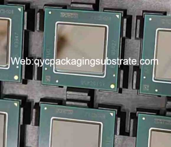
Process flow ic package substrate fabrication
What is IC Package Substrate Fabrication?
IC Package Substrate Fabrication is a key manufacturing process dedicated to creating the substrate for integrated circuit packaging. This process encompasses multiple steps and technologies, with the goal of producing packaging substrates that are high-performance, reliable, and adaptable to different applications.
IC Package Substrate Fabrication is a highly complex process designed to produce substrates for packaging integrated circuits. Basic concepts involve material selection, process flow and the application of innovative technologies. The core of the process is to build the substrate into a packaging structure that meets high-performance requirements through a series of steps.
Through IC Package Substrate Fabrication, we are able to customize the physical and electrical characteristics of the substrate to suit different packaging needs. This personalized manufacturing process allows the substrate to adapt to various application scenarios, thereby promoting the innovation and development of integrated circuit technology in multiple fields.
In general, IC Package Substrate Fabrication is not only a manufacturing process, but also a key technology that provides a solid foundation for the progress of the modern electronics industry.
Overview of the process flow of IC Package Substrate Fabrication
IC Package Substrate Fabrication is a complex process involving multiple critical steps, each of which has a profound impact on the performance and reliability of the final package substrate. The following are the general process steps of this process and their criticality:
The initiation of the manufacturing process begins with meticulous material preparation, encompassing the careful selection and conditioning of various elements such as substrate materials, metal foils, and other auxiliary materials. The precision and quality at this initial stage are intricately linked to the stability of subsequent processes and ultimately influence the reliability of the end product.
PCB manufacturing: Printed circuit board (PCB) manufacturing is the basis of the entire process. In this step, the basic circuit structure is formed through techniques such as printing and chemical etching, which determines the layout and connection methods of the final substrate.
Copper foil bonding: Copper foil is a key component of IC Package Substrate, which is bonded to the substrate through an bonding process. This step ensures that the foil is tightly bonded to the substrate, providing good electrical connection and thermal performance.
High-density interconnect technology (HDI): HDI technology plays a key role in improving substrate density and performance. By using microscopic holes, thin films and stacked layers, HDI technology can enable more connections in a limited space and support advanced electronic devices.
Material Preparation’s Influence: The reliability and performance of the substrate are directly shaped by the careful selection and quality of materials. Utilizing high-quality, versatile materials is crucial to guarantee the success of the process.
The layout in PCB design and manufacturing holds a pivotal influence on circuit performance and connectivity. A thoughtful and well-executed layout has the potential to optimize signal transmission, minimize interference, and guarantee the stability of the final product. In essence, the intricacies of PCB manufacturing significantly impact the arrangement and efficiency of the circuit connections, underscoring the importance of a judicious design process.
The importance of copper foil bonding: Copper foil bonding directly affects electrical conductivity and heat dissipation performance. A strong bonding process ensures a good electrical connection while helping to dissipate heat and improve device reliability.
The advancement of HDI technology: The use of HDI technology can provide more connections in a limited space and provide more possibilities for advanced electronic devices. Its improvement in substrate performance is the driving force for the continuous advancement of packaging substrate technology.
Taken together, the process flow overview of IC Package Substrate Fabrication highlights the criticality of each step. These steps are interconnected and jointly affect the quality and performance of the final packaging substrate. Emphasizing quality control and technological innovation at every step is key to ensuring the success of the process.
Key steps in the IC Package Substrate Fabrication process flow
Introduce the types and properties of materials required
During the early phases of IC Package Substrate Fabrication, a diverse array of materials comes into play, encompassing substrates, insulating materials, and metal foils. Each material brings forth distinctive electrical, insulating, and thermal conductivity properties, constituting crucial factors that significantly impact the performance of electronic devices.
Emphasize the importance of material selection to the manufacturing process
Material selection directly affects the performance and reliability of the final packaging substrate.
In-depth analysis of material properties to meet circuit requirements while considering process cost and sustainability.
Printed circuit board (PCB) manufacturing
The production of PCB usually includes steps such as raw material cutting, pattern etching, printing conductive materials, and coating of insulating layers.
During the manufacturing process, high-precision processes are required to ensure the accuracy and stability of the circuit.
As the main body of the packaging substrate, PCB carries and connects various chips and electronic components.
Properly designed PCB structure is critical to the performance and reliability of electronic devices.
Copper foil bonding
Copper foil bonding is a critical step in the packaging substrate process and involves bonding a copper foil layer to the substrate surface.
The selection and implementation of bonding technology is critical for signal transmission, thermal conductivity and mechanical stability in the process.
Explain its importance in the manufacturing process
Copper foil bonding directly affects the electrical and thermal conductivity of the packaging substrate, and has a direct impact on the performance and heat dissipation effect of electronic devices.
High Density Interconnect Technology (HDI)
HDI technology enables higher device density by adding more connections to the same or smaller area.
The widespread application of HDI in current electronic devices has improved the functionality and performance of packaging substrates.
The application of HDI can achieve shorter signal transmission paths, higher communication bandwidth, and improve the overall performance level of electronic devices.
Through HDI technology, more refined design and manufacturing of packaging substrates can be achieved to meet the needs of advanced electronic products.
Through the above key steps, IC Package Substrate Fabrication ensures high performance, high reliability and high-density integration of the packaging substrate. This process plays a vital role in the field of modern electronics, driving the continuous innovation and development of electronic devices.
The relationship between process flow and IC Package Substrate Fabrication
In the IC Package Substrate Fabrication process, the process flow plays a vital role, directly affecting the quality and performance of the final packaging substrate. The following are key aspects that are closely related to the process flow and IC Package Substrate Fabrication:
Every step in the manufacturing process has a profound impact on the quality of IC Package Substrate Fabrication. First, the material preparation stage determines the physical and electrical properties of the substrate. Selecting appropriate materials, such as high-quality insulation and highly conductive copper foil, is critical to ensuring substrate reliability and performance.
The printed circuit board (PCB) manufacturing process is one of the key steps in the manufacturing process. The design and manufacturing quality of PCB directly determines the hierarchical structure and wiring density of the packaging substrate. A high-quality PCB provides good electrical performance and lays a solid foundation for subsequent process steps.
The copper foil bonding stage also has a profound impact on the quality of IC Package Substrate Fabrication. Precise copper foil bonding technology ensures stable and reliable conductive properties, thereby improving overall package efficiency.
The application of high-density interconnect technology (HDI) is critical to substrate performance. Through HDI technology in the manufacturing process, higher density wiring can be achieved, improving the signal transmission rate and overall performance of the substrate.
Optimization of the manufacturing process is crucial to improving the efficiency of IC Package Substrate Fabrication. By adopting advanced manufacturing technology, the production cycle can be shortened, resource waste reduced, and product consistency and quality improved.
Innovative manufacturing processes can reduce production costs and make packaging substrates more competitive. By introducing automation and digital technology, the flexibility of the production line can be improved to adapt to different specifications and requirements, thereby better meeting market demand.
Optimizing manufacturing processes can also improve sustainable practices. Reducing the waste of energy and raw materials and using environmentally friendly materials are all goals of process optimization and contribute to the sustainable development of the electronics field.
While constantly pursuing innovation, optimization of process flow is a key part of achieving efficient, high-quality, and sustainable packaging substrate manufacturing. By continuously improving the manufacturing process, we can better adapt to rapidly changing market demands and promote progress in the entire electronics field.
Full text overview of IC Package Substrate Fabrication
IC Package Substrate Fabrication plays a pivotal role in the manufacturing process of integrated circuits (ICs), ensuring the efficient and precise creation of substrate materials for electronic devices. This process involves a series of crucial steps that contribute to the final quality and performance of the packaged ICs.
The significance of IC Package Substrate Fabrication lies in its ability to lay the foundation for the entire integrated circuit packaging process. Starting with material preparation and extending through printed circuit board (PCB) manufacturing, copper foil bonding, and high-density interconnect (HDI) technologies, each step holds paramount importance. The selection and preparation of materials, the intricacies of PCB manufacturing, and the precision in copper foil bonding all contribute to the overall success of the fabrication process.
The fabrication process acts as the backbone of IC packaging, influencing the structural integrity and electrical performance of the final product. The careful execution of each step ensures the creation of a robust and reliable substrate, critical for the seamless integration of electronic components.
Continuous innovation and refinement within IC Package Substrate Fabrication play a pivotal role in propelling the electronic packaging field forward. In a dynamic technological landscape, maintaining a leading position in manufacturing processes is essential. The incorporation of novel materials, improved bonding techniques, and state-of-the-art HDI technologies contributes to the evolution of substrates that are not only more efficient but also higher-performing.
This commitment to innovation not only elevates the quality of the fabrication process but also steers the industry towards heightened sustainability. Underscoring the significance of sustainable practices and environmentally friendly manufacturing processes is imperative for the enduring health of the electronic industry. Prioritizing eco-friendly approaches ensures that the fabrication process aligns with global initiatives toward a more sustainable and environmentally conscious future.
In conclusion, the IC Package Substrate Fabrication process serves as the cornerstone of integrated circuit manufacturing. Its meticulous steps and attention to detail ensure the creation of high-quality substrates, essential for the seamless functioning of electronic devices. As technology continues to advance, a commitment to continuous innovation and optimization becomes paramount, propelling the industry forward and fostering a sustainable future for electronic manufacturing.