 Professional Flip-Chip Packaging Substrate Supplier

What exactly is a packaging substrate?
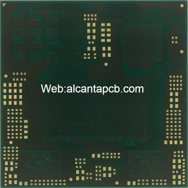
Packaging substrate manufacturing. We have produced many kinds of BGA substrate, the smallest via holes are 50um,the smallest pitch is 100um.and the Microtrace are 9um. Spacing are 9um too.
In the field of PCB (Printed Circuit Board) engineering, packaging substrate (Packaging Substrate) significantly plays a key technical role. Packaging substrate can be regarded as an indispensable technology, which plays a vital role in supporting and connecting chips in the design and manufacturing of electronic devices. In this article, we will delve into the importance of the packaging substrate and its function and value in the overall electronic system.
The packaging substrate ensures that the chip is securely placed on the circuit board by providing a reliable platform and connected to other components through its internal electrical connection points. This is not just a simple physical support, but also provides a solid foundation for the transmission of electronic signals.
Another key role packaging substrates play in electronic devices is in thermal management. As the chips work, they generate a considerable amount of heat. The cleverness of the packaging substrate design is to effectively conduct and dissipate this heat to keep the chip within a suitable operating temperature range. This thermal management is crucial to ensure stable operation of the chip for a long time, which directly affects the performance and life of electronic equipment.
The packaging substrate provides the necessary mechanical support to the chip through the solid design of its structure, effectively protecting the chip from these external factors.
Taken together, the status of packaging substrates in electronic equipment cannot be underestimated. By making full use of different types of packaging substrates, such as BGA (Ball Grid Array) and LGA (Land Grid Array), engineers can optimize according to specific application requirements, thereby promoting continuous innovation in electronic technology. Therefore, packaging substrate, as a core component of PCB engineering, plays a vital role in promoting the development and performance improvement of electronic equipment.
Packaging Substrate
What is the function of the packaging substrate?
In PCB (Printed Circuit Board) engineering, packaging substrate (Packaging Substrate) is an indispensable and important component in electronic equipment. The packaging substrate is responsible for a number of vital functions, which not only directly affect the performance of the chip, but are also related to the reliability and stability of the entire electronic device.
First, the packaging substrate plays an important electrical connection function in electronic devices. As a bridge between the chip and other electronic components, the packaging substrate ensures the efficient transmission of electrical signals. Through precision-designed wires and connection points, the packaging substrate enables the rapid and stable exchange of information between various components to achieve normal operation of the device. The superiority of this electrical connection makes packaging substrates an indispensable and critical component of modern electronic devices.
Secondly, heat dissipation is another key function of the packaging substrate. As the heat generated by the chip increases during operation, the packaging substrate helps to quickly transfer the heat energy to the surrounding environment through a properly designed heat dissipation structure. This effectively maintains the chip within a safe operating temperature range, preventing performance issues and damage caused by overheating. The heat dissipation design of packaging substrates in electronic devices is critical to ensuring long-term stable operation of the device.
Finally, the packaging substrate provides critical mechanical support to the chip. Through precision manufacturing and design, the packaging substrate can firmly support the chip and prevent it from vibration, impact or mechanical damage from the external environment. This mechanical support not only helps extend the life of the chip but also ensures device reliability under a variety of conditions. The structure and material selection of the packaging substrate directly affects the effectiveness of the mechanical support it provides, so precision during the manufacturing process is particularly critical.
Overall, the packaging substrate, as the core component of electronic equipment, ensures the normal operation of the chip and the reliability of the equipment through superior electrical connections, effective heat dissipation design and solid mechanical support. In the ever-evolving field of electronic technology, the research, development and innovation of packaging substrates will continue to promote the performance improvement and functional expansion of electronic equipment.
What are the different types of packaging substrates?
In PCB (Printed Circuit Board) engineering, packaging substrate (Packaging Substrate) is an indispensable and important component in electronic equipment. The packaging substrate is responsible for a number of vital functions, which not only directly affect the performance of the chip, but are also related to the reliability and stability of the entire electronic device.
First, the packaging substrate plays an important electrical connection function in electronic devices. As a bridge between the chip and other electronic components, the packaging substrate ensures the efficient transmission of electrical signals. Through precision-designed wires and connection points, the packaging substrate enables the rapid and stable exchange of information between various components to achieve normal operation of the device. The superiority of this electrical connection makes packaging substrates an indispensable and critical component of modern electronic devices.
Secondly, heat dissipation is another key function of the packaging substrate. As the heat generated by the chip increases during operation, the packaging substrate helps to quickly transfer the heat energy to the surrounding environment through a properly designed heat dissipation structure. This effectively maintains the chip within a safe operating temperature range, preventing performance issues and damage caused by overheating. The heat dissipation design of packaging substrates in electronic devices is critical to ensuring long-term stable operation of the device.
Finally, the packaging substrate provides critical mechanical support to the chip. Through precision manufacturing and design, the packaging substrate can firmly support the chip and prevent it from vibration, impact or mechanical damage from the external environment. This mechanical support not only helps extend the life of the chip but also ensures device reliability under a variety of conditions. The structure and material selection of the packaging substrate directly affects the effectiveness of the mechanical support it provides, so precision during the manufacturing process is particularly critical.
Overall, the packaging substrate, as the core component of electronic equipment, ensures the normal operation of the chip and the reliability of the equipment through superior electrical connections, effective heat dissipation design and solid mechanical support. In the ever-evolving field of electronic technology, the research, development and innovation of packaging substrates will continue to promote the performance improvement and functional expansion of electronic equipment.
Packaging Substrate
What is the relationship between packaging substrate and IC packaging?
In PCB engineering, there is a close relationship between packaging substrate and IC packaging, which involves the key position of IC (Integrated Circuit) packaging technology. IC packaging technology plays a vital role in the design of modern electronic equipment, and different chip packaging technologies, such as CSP (Chip Scale Package) and QFN (Quad Flat No-leads), have a direct impact on the performance and size of electronic equipment. And far-reaching impact.
The criticality of IC packaging technology
IC packaging stands as a crucial process in transforming integrated circuit chips into a usable form for electronic devices. The significance of this technology is evident in its capacity to shield the chip from external environmental hazards, establish essential electrical connections, and assist in managing the heat generated by the chip to a certain extent. Within PCB engineering, the choice of IC packaging directly influences the overall performance, stability, and dimensions of the electronic device.
The impact of different packaging technologies
CSP (Chip Scale Package) and QFN (Quad Flat No-leads) are two common chip packaging technologies. CSP packaging is a miniaturized and lightweight packaging method. Its goal is to package the chip to a size similar to the chip itself. This packaging method can significantly reduce the overall size of electronic equipment, improve the integration of the equipment, and help achieve thinner, lighter and more portable products.
In contrast, the QFN package connects the chip directly to the PCB through a more compact electrical connection and a flat appearance design, omitting the need for traditional pins. This packaging method reduces the overall size to a certain extent and provides higher heat dissipation efficiency, which is suitable for scenarios that have strict requirements on size and heat dissipation performance.
Performance and size trade-offs
When choosing an IC packaging technology, engineers need to make a trade-off between performance and size. CSP packaging provides the possibility of miniaturization, but may have a certain impact on heat dissipation performance. QFN packaging emphasizes heat dissipation performance, but may sacrifice product miniaturization to a certain extent.
Therefore, the packaging substrate plays a key support and connection role in IC packaging. The design of the packaging substrate needs to take into account the requirements of different packaging technologies for electrical connection, heat dissipation and mechanical support to ensure that the entire electronic device achieves the best balance between performance and size.
By having an in-depth understanding of different chip packaging technologies, engineers can better choose the packaging method suitable for their design needs, thereby achieving the best overall performance in PCB engineering. This understanding helps drive innovation in electronic devices to make them more compact, efficient and reliable.
What is the difference between packaging substrate and PCB?
Although packaging substrates (Packaging Substrate) and printed circuit boards (PCBs) are both indispensable core components of electronic devices, they have some key differences in structure and function. In this article, we will provide an in-depth introduction to the differences between PWBs and PCBs, and discuss the similarities and differences in motherboard (Motherboard), packaging substrate, substrate-like PCB (SLP), and HDI packaging.
Before delving into the distinctions between PWBs and PCBs, it’s essential to grasp their definitions. A Printed Circuit Board (PCB) is a flat panel that facilitates the interconnection of electronic components. Through a design involving copper foil, insulating materials, and stacked layers, it establishes electrical connections. On the other hand, a Packaging Substrate is primarily geared towards supporting and packaging chips to ensure their proper functioning in electronic devices.
Now, turning our attention to the motherboard, a significant component in this context, it represents a sizable printed circuit board responsible for housing the core elements of an electronic device, encompassing the central processing unit (CPU), memory, and other crucial components. In contrast, the packaging substrate is more narrowly focused on the packaging and interconnection of chips, providing them with electrical connections, mechanical support, and facilitating heat dissipation functions.
Another area to focus on is Substrate-like PCB (SLP) and HDI packaging. Substrate-like PCB is a printed circuit board that uses a structure similar to a packaging substrate, but has a more complex manufacturing process. In contrast, HDI packaging (High-Density Interconnect) emphasizes high-density interconnection and achieves smaller package size through finer processes. Both of them present unique characteristics in design and application, and are more advanced than traditional PCBs.
In general, packaging substrates focus on the packaging and connection of chips, emphasizing the reliability and performance of electrical connections, while taking into account heat dissipation and mechanical support. PCB is broader, including various types of circuit boards, covering motherboards, SLP, HDI packaging and other aspects, aiming to meet the needs of different electronic devices.
Overall, although packaging substrates and PCBs both play critical roles in electronic devices, they have significant differences in design, functionality, and applications. By gaining a deeper understanding of their similarities and differences, we can better understand the complex and sophisticated engineering structures behind electronic devices.
What are the main structures and production technologies of packaging substrates?
Understanding the structure of a packaging substrate is critical to uncovering its functionality. Packaging substrates play a key role in electronic devices by connecting and supporting chips. The structure of the packaging substrate and related manufacturing technologies will be introduced in detail below, including improved HDI manufacturing technology and semi-additive methods.
Package substrate structure
The structure of the packaging substrate is complex and diverse, and its main components involve conductors, insulating layers and possible additional components. First, the conductor layer is a key component in the package substrate and is used for electrical connections. These conductors, usually made of copper, are manufactured using sophisticated processes to create complex circuit patterns that provide good electrical connections to the chips.
In the packaging substrate design, supplementary components like capacitors, inductors, and others may be incorporated strategically to amplify the circuit’s performance. These elements are seamlessly integrated into the packaging substrate’s structure, contributing to a more streamlined and efficient overall circuit system.
HDI manufacturing technology
HDI (High-Density Interconnect) manufacturing technology is an important innovation in the field of packaging substrates. Through HDI technology, more electrical connections can be achieved in a limited space, thereby improving the integration of circuits. Key to this technology is the use of advanced processes such as laser drilling and film-sealed holes to enable smaller, denser conductor layouts.
Improvements in HDI manufacturing technology have made packaging substrates more suitable for advanced electronic devices such as smartphones and high-performance computers. It provides higher signal transmission rates and smaller circuit board size, bringing greater flexibility to the design of electronic products.
Semi-additive method
The semi-additive method is another key technology for packaging substrate manufacturing. In this approach, manufacturers add metal to the conductor layer in a semi-additive manner to create the desired circuit pattern. Compared with the traditional full addition method, this reduces material waste and improves production efficiency.
The semi-additive method stands out for its ability to lower manufacturing costs and decrease raw material requirements. This bears significant implications for high-volume production, offering an economical and sustainable solution for the electronics industry.
By combining HDI manufacturing technology and semi-additive methods, packaging substrates can achieve a more efficient production process while maintaining high performance.
Overall, the structure and manufacturing technology of the packaging substrate are important components in PCB engineering.
Frequently Asked Questions (FAQs) for Package Substrates
What role does the packaging substrate play in PCB engineering?
In PCB engineering, the packaging substrate assumes several crucial functions. Initially, it facilitates efficient signal transmission between the chip and other electronic components by establishing essential electrical connections. Additionally, the packaging substrate plays a pivotal role in dissipating the heat generated by the chip, thereby maintaining the chip within a safe operating temperature range. This dual function enhances the overall reliability and performance of the device. Lastly, the packaging substrate provides indispensable mechanical support to the chip, shielding it from potential damage arising from the external environment.
What are the types of packaging substrates?
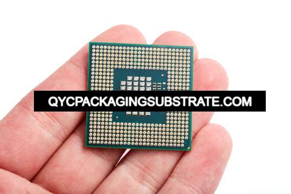
A variety of packaging substrates exists, with common examples being BGA (Ball Grid Array) and LGA (Land Grid Array). Each type possesses distinct characteristics, making them suitable for specific application scenarios. The careful selection of the appropriate packaging substrate type is crucial, as it significantly influences the performance and reliability of the overall electronic device.
What is the relationship between packaging substrate and IC packaging?
IC (Integrated Circuit) packaging technology is directly related to the packaging substrate. Different chip packaging technologies, such as CSP (Chip Scale Package) and QFN (Quad Flat No-leads), have a direct impact on the performance and size of the device. Reasonable selection of IC packaging technology and packaging substrate type will help optimize circuit layout and overall device design.
What is the difference between packaging substrate and PCB?
While both packaging substrates and PCBs are core components of electronic devices, they have some key differences. PCB is the basis of the entire circuit board, while the packaging substrate is more focused on supporting and connecting chips. Understanding the differences between them helps engineers better design and optimize electronic devices.
What are the production technologies for packaging substrates?
The production technology of packaging substrates covers many aspects, including structural design and manufacturing processes. Understanding its main structure and manufacturing technologies, such as improved HDI manufacturing technology and semi-additive methods, can help optimize the performance and manufacturability of packaging substrates.
Full text overview of packaging substrates
The Packaging Substrate, a crucial component in contemporary electronic equipment, holds a direct correlation between its design and manufacturing and the overall performance and stability of the equipment. A comprehensive comprehension of the role, types, and interplay of packaging substrates with other components represents a pivotal step in grasping the intricacies and innovations within PCB engineering.
The significance of packaging substrates within electronic devices is undeniable. Among its functions is the facilitation of electrical connections to ensure efficient signal transmission between chips and other electronic components. Simultaneously, the packaging substrate serves a vital role in heat dissipation, effectively managing the thermal output from the chip and maintaining it within a safe operating temperature range. Furthermore, the packaging substrate offers mechanical support for the chip, shielding it from potential damage originating from the external environment.
This enables engineers to select the most appropriate packaging substrate type based on device requirements, maximizing its performance.
Directly related to IC packaging is chip packaging technology, including CSP (Chip Scale Package) and QFN (Quad Flat No-leads). These technologies directly impact the performance and size of electronic devices, providing engineers with flexibility and choice in their designs.
There are important differences between packaging substrates and PCBs. The article will introduce the differences between PWBs and PCBs, as well as the similarities and differences in motherboard, packaging substrate, substrate-like PCB (SLP) and HDI packaging. A deeper understanding of these differences can help engineers better select and optimize circuit board designs.
A comprehensive comprehension of the structure and manufacturing methodologies employed in packaging substrates holds paramount significance for engineers. This article aims to intricately detail the architecture and manufacturing technologies associated with packaging substrates, spotlighting advancements in High-Density Interconnect (HDI) manufacturing technology and the semi-additive method. The continual evolution and innovation in these technologies serve as driving forces behind the enhanced development of electronic devices, contributing to heightened performance and reliability.
Broadly speaking, the packaging substrate constitutes the central component responsible for connecting and supporting the chip, exerting a pivotal influence on the overall performance and reliability of the device. A profound understanding of every facet of packaging substrates enables a nuanced appreciation of the intricacies and innovation inherent in PCB engineering.