 Professional Flip-Chip Packaging Substrate Supplier

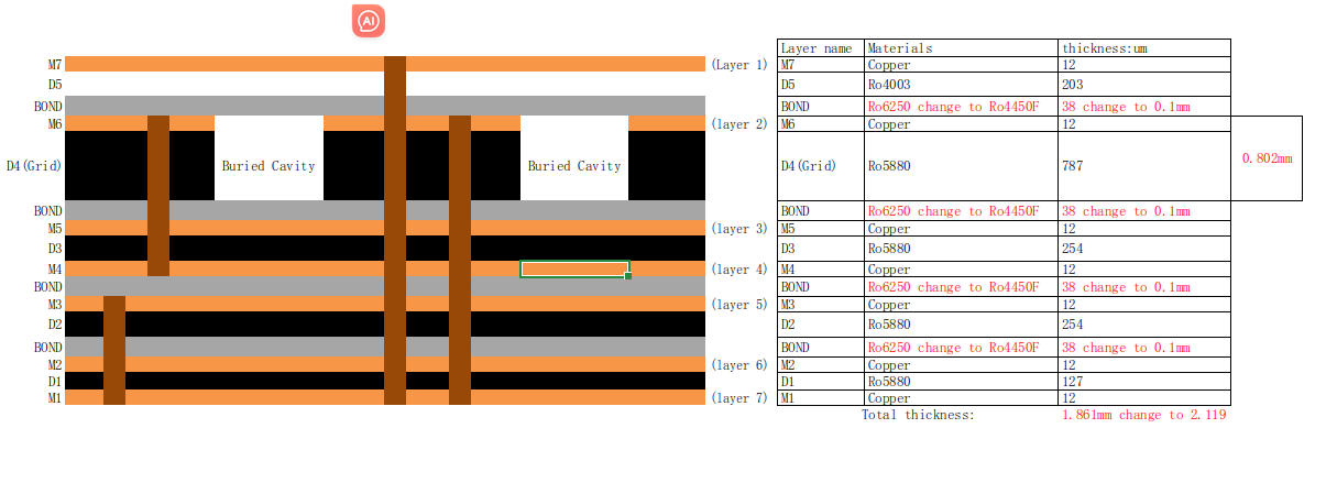
RF Cavity PCB manufacturing, Step RF Cavity PCBs and Mixed dielectric material RF Cavity PCBs Vendor, we offer many types Cavity PCBs, Step Cavity PCBs, Embedded Cavity PCBs from 4 layer to 50 layers.
Cavity PCB is a printed circuit board with a cavity structure, which is characterized by hollows inside the board to accommodate electronic components. This design not only provides higher circuit density and performance, but also provides better thermal dissipation and electromagnetic compatibility. Cavity PCB plays a key role in electronic equipment, providing stable electronic connections and support for various applications, especially in high frequency, microwave and radio frequency applications.
How to design Cavity PCB?
Designing a Cavity PCB is a complex and critical process that requir
es the consideration of multiple factors to ensure the performance and reliability of the final product. Here are the key principles and steps to consider when designing Cavity PCB:
Cavity design and layout: First, the location and size of the cavity need to be determined based on the overall layout of the circuit board. When designing the cavity, make sure it is large enough to accommodate the required components and does not adversely affect the stability and structure of the board.
EMI and RFI protection: In Cavity PCB design, electromagnetic interference (EMI) and radio frequency interference (RFI) protection measures need to be considered. Through proper layout and shielding design, interference between circuit boards can be reduced and the system’s anti-interference ability improved.
Thermal Management: For high-power electronic devices, thermal management is one of the important factors that must be considered during the design process. In Cavity PCB design, it is necessary to rationally layout heat sinks, heat pipes and other heat dissipation components to ensure the stable operation of the circuit board and extend the service life of the components.
Material Selection: In Cavity PCB design, choosing the right material is critical to the performance and reliability of the board. Factors such as the dielectric constant, thermal conductivity, and mechanical strength of the material need to be considered and selected according to specific application scenarios.
Routing and impedance control: When designing Cavity PCB, special attention needs to be paid to routing and impedance control. Reasonable wiring design can reduce loss and interference during signal transmission, while strict impedance control can ensure signal quality and stability.
Process and manufacturing feasibility: Finally, when designing Cavity PCB, the feasibility and cost-effectiveness of the manufacturing process need to be considered. It is necessary to select the appropriate manufacturing process and ensure that the design meets the process requirements for smooth production and assembly.
To sum up, designing Cavity PCB requires comprehensive consideration of cavity design, EMI and RFI protection, thermal management, material selection, wiring and impedance control, as well as process and manufacturing feasibility. Through reasonable design and careful planning, the performance and reliability of Cavity PCB can be ensured to meet the needs of specific applications.
RF Cavity PCB
What is the manufacturing process of Cavity PCB?
In the process of manufacturing Cavity PCB, a series of precise processes and steps are involved to ensure that the final product is of high quality and reliability. The manufacturing process of Cavity PCB will be introduced in detail below, including key steps and specific processes.
Before Cavity PCB can be manufactured, detailed design work first needs to be carried out. This includes determining the size, layout and cavity locations of the PCB, as well as determining the required materials and special processing requirements. After the design is completed, the required materials need to be prepared, including substrates, circuit diagram layers, special substrate materials, etc.
Next comes the process of printing the circuit layer onto the substrate. This step includes coating of light-sensitive materials, exposure to photolithography, etching and other steps to form circuit lines on the PCB. For Cavity PCB, special attention should be paid to the circuit layout around the cavity to ensure that the edges of the cavity are clear and the circuit lines are not affected.
In Cavity PCB, the design and manufacturing of the cavity are crucial steps. Generally, the cavity is manufactured by mechanical processing or film coating. Mechanical processing often includes CNC machining and laser cutting to ensure that the size and shape of the cavity meet the design requirements. Thin film coating adds a special film to the circuit layer, and then forms a cavity through chemical etching and other steps.
In addition to cavity manufacturing, Cavity PCB manufacturing also involves some special processing techniques to meet specific application requirements. This may include deep hole drilling, metallization, special overlays, etc. The selection and application of these processes need to be determined based on specific design requirements and application scenarios.
Quality control and testing are crucial aspects of the entire manufacturing process. This includes checking the quality of materials, monitoring key parameters during the manufacturing process, and comprehensive testing and inspection of the final product. Only by ensuring product quality and reliability can we meet customer needs and requirements.
The manufacturing process of Cavity PCB involves multiple key steps and precision processes, requiring a high degree of professional knowledge and technology. Through strict quality control and testing, as well as continuous technological innovation, we can ensure the manufacture of Cavity PCB products with high quality, reliability and superior performance to meet the needs of different application scenarios.
What is the manufacturing process of Cavity PCB?
The manufacturing process of Cavity PCB is a complex and delicate process that requires multiple critical steps to ensure the quality and performance of the final product. The material preparation and processing steps required to manufacture Cavity PCB will be introduced in detail below, as well as the special processing technology for designing and manufacturing the cavity in Cavity PCB.
Before manufacturing Cavity PCB, you first need to prepare suitable substrate materials and film materials. Commonly used substrate materials include FR-4 fiberglass composites and high-frequency materials, while thin film materials are often used to form the cavities of PCBs. Next, through steps such as cutting and processing, the substrate material and film material are processed and prepared according to the design requirements for the subsequent PCB manufacturing process.
Designing and manufacturing the cavities in Cavity PCB is one of the key steps in the Cavity PCB manufacturing process. During the design stage, engineers need to determine the size, shape, and location of the cavity based on the product’s requirements and specifications, and reasonably lay out the relationship between the cavity and other circuit components. In the manufacturing stage, special processing techniques and equipment, such as CNC milling machines or laser cutting machines, are used to precisely process the PCB board to form a cavity structure. In addition, attention should be paid to the smoothness and flatness of the cavity edges to ensure the quality and stability of the cavity.
In the process of manufacturing the cavity of Cavity PCB, some special processing techniques need to be paid attention to to ensure the accuracy and quality of the cavity. The first is dimensional control during processing, which needs to ensure that the size and shape of the cavity are consistent with the design requirements. Second is temperature and humidity control during processing to prevent material deformation or damage. In addition, it is necessary to use suitable cutting tools and cutting tools to ensure precise and stable processing of PCB boards. Finally, after the processing is completed, strict quality inspection and testing are required to ensure that the quality and performance of the cavity meet the design requirements.
To sum up, the process of manufacturing Cavity PCB involves multiple key steps and special processing techniques, and each link needs to be strictly controlled to ensure the quality and performance of the final product.
How much does Cavity PCB cost?
The cost of Cavity PCB is an important factor that needs to be considered in depth during the design and manufacturing process. Understanding the factors that affect Cavity PCB costs and how to evaluate and optimize these costs is critical to manufacturing high-quality Cavity PCBs.
First, let’s look at the main factors that affect Cavity PCB cost:
Design complexity: The design complexity of Cavity PCB directly affects the manufacturing cost. Complex designs may require more processing steps and special processes, increasing costs.
Material selection: The type and quality of materials used in Cavity PCB will also affect its cost. High-performance specialty materials are usually more expensive, while some low-cost materials may sacrifice certain performance and reliability.
Production volume: The size of production volume is directly related to cost. Generally speaking, high-volume production can reduce unit costs, while small-volume production may increase costs.
Manufacturing process: Different manufacturing processes will have an impact on the cost of Cavity PCB. For example, some special processing techniques may require higher technical requirements and equipment investment, thereby increasing costs.
After understanding the factors that affect cost, how to evaluate and optimize the cost of Cavity PCB?
Design optimization: Reducing costs by optimizing the design is an effective method. Simplifying the design and reducing complexity can reduce manufacturing costs and improve production efficiency.
Material Selection: Choosing the right materials is critical to controlling costs. Choosing materials with appropriate performance and affordable prices based on actual needs can reduce costs without affecting product quality.
Improve production efficiency: Taking effective production process and process control measures can improve production efficiency and thereby reduce costs. Properly arranging production plans to reduce scrap rates and production cycles can reduce manufacturing costs.
Reasonable negotiation: Reasonable negotiation and consultation with suppliers can reduce raw material procurement costs and obtain better price advantages.
In summary, understanding the factors that affect Cavity PCB cost and taking corresponding measures for evaluation and optimization can help manufacturers reduce costs, improve competitiveness, and provide more cost-effective products.
What material is Cavity PCB made of?
Cavity PCB (cavity PCB) is a special type of printed circuit board widely used in the electronic field. The materials selected during its design and manufacturing process are crucial to its performance and reliability. Let’s take a closer look at the commonly used Cavity PCB materials and the factors to consider when choosing a material.
FR-4 (glass fiber reinforced epoxy resin): FR-4 is one of the most common PCB substrates. It has good insulation properties and mechanical strength and is suitable for Cavity PCB manufacturing in most general application scenarios.
PTFE (Polytetrafluoroethylene): PTFE has excellent high-frequency characteristics and high-temperature resistance, and is often used in Cavity PCB manufacturing that requires high-frequency signal transmission and works in extreme environments.
RF-35 (polyimide): RF-35 material has excellent high-frequency performance, chemical resistance and thermal stability, and is suitable for applications such as wireless communications that require strict high-frequency characteristics.
Metal substrate (such as aluminum substrate, copper substrate): Metal substrate has good thermal conductivity and heat dissipation effect, and is often used in Cavity PCB manufacturing that needs to handle high power and heat, such as LED lighting, power modules and other fields.
Composite materials: Composite materials combine the advantages of different types of materials, such as polyimide/glass fiber composite materials, which provide good insulation properties and mechanical strength and are suitable for Cavity PCB manufacturing in a variety of complex environments.
Factors to consider when choosing materials
Working environment and application scenarios: Consider the environmental conditions in which Cavity PCB will be used, including temperature, humidity, chemical exposure, etc., and select materials with appropriate properties.
Signal transmission requirements: If Cavity PCB needs to handle high-frequency signals, materials with good high-frequency characteristics should be selected, such as PTFE or polyimide.
Thermal management needs: If the Cavity PCB needs to handle high power or heat, materials with good thermal conductivity should be selected, such as metal substrates or composite materials with excellent heat dissipation properties.
Manufacturing complexity and cost: Consider the material’s workability, cost, and special processes that may be involved in the manufacturing process to select materials that fit your manufacturing budget and requirements.
Reliability and long-term stability: Choose materials with good reliability and long-term stability to ensure the performance and reliability of Cavity PCB during use.
To sum up, the material selection of Cavity PCB is crucial to its performance and reliability. When selecting materials, factors such as the working environment, signal transmission requirements, thermal management needs, manufacturing complexity and cost need to be comprehensively considered to ensure that the final Cavity PCB can meet the needs of the design and application.
Who makes Cavity PCB?
When manufacturing Cavity PCB, choosing the right manufacturer is crucial. The choice of manufacturer directly affects product quality, delivery time and service level. Here is some information on how to choose the right manufacturer and who our company is.
As a professional Cavity PCB manufacturer, we are committed to providing customers with high-quality products and services. We have advanced production equipment and technical teams that can meet the needs of various complex projects. The following are the services and advantages provided by our company:
Technical strength: We have an experienced engineering team with advanced manufacturing technology and rich industry experience, able to provide professional technical support and solutions.
Quality Assurance: We strictly implement the quality management system and strictly control every link from raw material procurement to production and manufacturing to ensure that the products meet high quality standards.
Flexible production: We have flexible production lines and quick response capabilities, and can customize production according to customer needs to meet the special requirements of different customers.
Quality service: We focus on communication and cooperation with customers, providing timely technical support and after-sales service to ensure customer satisfaction and smooth project progress.
By choosing us as Cavity PCB manufacturer, you will enjoy high-quality products, excellent service and competitive prices. We look forward to cooperating with you and developing together.
Five Characteristics of Great Customer Service
Professional knowledge and experience: A quality Cavity PCB manufacturing company should have extensive professional knowledge and experience and be able to understand customer needs and provide customized solutions. They should be familiar with different types of Cavity PCB design and manufacturing processes and be able to provide professional advice and guidance according to customer requirements.
Prompt response: First-class customer service means quick and timely response to customer inquiries and needs. Manufacturing Cavity PCB is usually a complex process, and customers may require timely technical support or solutions. Therefore, companies should maintain open lines of communication and be able to respond promptly when customers have questions or needs.
Customized Solutions: Each customer’s needs may be unique, so a quality Cavity PCB manufacturing company should be able to provide customized solutions to meet the customer’s specific needs. They should work closely with clients to understand their needs and requirements and tailor the most suitable solution for them.
Good Communication: Throughout the manufacturing process, good communication is key to ensuring customer satisfaction. Companies should be able to clearly communicate manufacturing progress and project status, and promptly communicate with customers any changes or delays that may impact the project. Additionally, they should be able to actively listen to customer feedback and make adjustments and improvements based on customer needs.
Through the above measures, customers can ensure a high-quality customer service experience and establish a long-term and stable cooperative relationship with Cavity PCB Manufacturing Company.
FAQS
What are the common challenges in designing a Cavity PCB?
Designing a Cavity PCB presents unique challenges, particularly in managing signal integrity, thermal dissipation, and mechanical stability. Ensuring proper alignment and compatibility with enclosure dimensions is also crucial. Designers must navigate these challenges while maintaining signal integrity and reliability.
How does the choice of materials impact Cavity PCB performance?
Material selection significantly influences Cavity PCB performance. High-frequency applications may require materials with low dielectric constants and loss tangents to minimize signal loss. Thermal management considerations may necessitate materials with high thermal conductivity. Understanding the properties of different materials is essential for optimizing Cavity PCB performance.
What are the key considerations for selecting a Cavity PCB manufacturer?
When selecting a Cavity PCB manufacturer, factors such as experience, technical capabilities, quality standards, and production capacity should be considered. It’s essential to choose a manufacturer with expertise in Cavity PCB fabrication and a proven track record of delivering high-quality products.
How can one ensure the reliability of Cavity PCBs in harsh environments?
Ensuring the reliability of Cavity PCBs in harsh environments requires robust design practices, proper material selection, and thorough testing. Conformal coating or encapsulation may be employed to protect against moisture, dust, and other contaminants. Additionally, reliability testing under simulated operating conditions can validate the performance of Cavity PCBs in real-world environments.