 Professional Flip-Chip Packaging Substrate Supplier

What is FCBGA package substrate?
Semiconductor FCBGA Package substrate Manufacturer. Advanced equipment and process technology support high layer substrate production.
FCBGA, or Flip-Chip Ball Grid Array, is a leading integrated circuit packaging technology. Its name comes from its key features: the chip is flip-packed and electrically connected to the substrate through a solder ball array. The introduction of this technology plays a key role in improving the performance and reliability of modern electronic equipment.
In FCBGA, the chip packaging method is different from the traditional method. A more compact packaging structure is achieved by flipping the chip directly, that is, with the back of the chip facing the substrate, and then connecting to the substrate through a solder ball array. This flipped design helps improve the electrical performance of the chip and reduce signal transmission delays, thereby enhancing overall work efficiency.
The solder ball array is another key component of the FCBGA. The design density and arrangement of solder balls have an important impact on the performance of the package. Through clever design, FCBGA can provide more input/output pins, providing greater development space for high-performance applications. This high-density connection method also helps adapt to the continuous pursuit of miniaturization and lightweight of modern electronic devices.
In addition to its basic concept, FCBGA is unique in its special position in integrated circuit packaging technology. When compared with other chip packaging technologies, FCBGA occupies a place in the IC packaging field with its flip-type design and solder ball connection advantages. The advantages of this packaging method make FCBGA widely used in high-performance computing, communication equipment and other fields that have strict requirements on electrical performance.
In general, FCBGA, as a representative of Flip-Chip Ball Grid Array, provides key support for the performance improvement and miniaturization development of modern electronic equipment through its advanced packaging technology. Its flip design and solder ball connection method make the chip layout more compact, while the high-density connection method provides more flexible options for high-performance applications. In the evolving electronics field, FCBGA’s status will continue to highlight its importance in integrated circuit packaging technology.
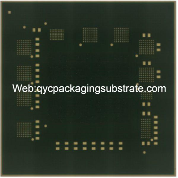
FCBGA package
What are the functions of FCBGA?
FCBGA (Flip-Chip Ball Grid Array) is not just a packaging technology, but a key tool in modern electronics, designed to provide excellent performance and flexibility. Let’s dive into the main features of FCBGA and understand how it improves chip performance by providing higher density and shorter signal paths, making it an ideal solution for high-performance applications.
Higher Density and Shorter Signal Paths
The design of FCBGA focuses on increasing the density of the chip, making full use of space by flipping the chip directly and connecting it to the substrate. This design allows for more input/output pins, providing the chip with greater connectivity than traditional packaging, allowing it to handle more data and tasks.
At the same time, FCBGA optimizes the response speed of the circuit by reducing the signal transmission delay. Traditional packaging forms may cause signal delays due to long signal paths, while FCBGA minimizes the signal transmission path by directly connecting the chip and the substrate, achieving faster data transmission.
More input/output pins
Through its unique design, FCBGA allows more input/output pins to be arranged in a limited space. This flexibility enables the chip to handle multiple tasks at the same time and provide more interfaces for complex electronic systems, thereby meeting the requirements for data exchange and processing capabilities in different application scenarios.
Ideal for high performance
Based on the above characteristics, FCBGA has become an ideal choice for high-performance applications. Whether in computer processors, graphics processing units or communications equipment, FCBGA can fully optimize system performance by providing higher integration and shorter signal paths. The widespread use of this packaging technology demonstrates its unique advantages in meeting the speed and performance requirements of today’s electronic devices.
Overall, FCBGA has successfully become a pioneer in high-performance electronic applications with its superior features, including higher density, shorter signal paths, and more input/output pins. It not only meets the needs of modern electronic equipment for compact, efficient, and high-performance packaging, but also provides electronic engineers with a flexible and reliable solution, promoting the continuous progress of electronic technology.
What are the different types of FCBGA?
FCBGA (Flip-Chip Ball Grid Array), as an advanced integrated circuit packaging technology, has many different types. These types have significant differences in the arrangement of the ball grid array and the arrangement density of the solder balls. A thorough understanding of these different types is critical to selecting the right package for a specific application.
First, let’s explore the different ball grid array arrangements of FCBGA. In the FCBGA package, the arrangement of the ball grid array directly affects the performance and application fields of the chip. One common type is a square arrangement, which distributes the solder balls evenly throughout the package and helps improve the reliability of the electrical connection. In addition, there are various methods such as spiral arrangement and double arrangement, each of which is optimized for specific design needs and application scenarios.
Secondly, the arrangement density of solder balls is another key factor. Different types of FCBGA have differences in the arrangement density of solder balls, which directly affects the number of pins and the power consumption performance of the package. The high-density solder ball arrangement can accommodate more pins, allowing the chip to handle more complex circuit designs and is suitable for high-performance computing and communication equipment.
Understanding the different types of FCBGA, we can better respond to different application needs. For example, in mobile devices that are sensitive to power consumption, FCBGAs with moderate solder ball density can be selected to balance performance and power consumption. For servers and network equipment that require larger pin counts and higher performance, FCBGAs with higher solder ball density can be selected.
Overall, the diversity of FCBGA provides engineers with the opportunity to flexibly choose in different application scenarios. By gaining an in-depth understanding of these different types, we can better understand their advantages and scope of application, thereby better meeting the design requirements of a specific project. While pursuing performance and reliability, choosing the right FCBGA type will play a key role in the field of electronic engineering.
What is the relationship between FCBGA and IC packaging?
In the field of modern integrated circuit packaging, the evolution of chip packaging technology has always been a key factor in promoting the performance improvement of electronic equipment. During this evolution, FCBGA (Flip-Chip Ball Grid Array) occupies a special position in IC packaging with its unique design and performance advantages, which is significantly different from other chip packaging technologies.
First, let’s take a deeper look at the classification of chip packaging technologies. Among many packaging technologies, traditional packaging methods include QFP (Quad Flat Package), SOP (Small Outline Package), etc., which use cable connections when connecting chips and substrates. However, FCBGA uses a unique design of flipping the chip and achieving electrical connections through a solder ball array, making it completely different from the traditional method.
The uniqueness of FCBGA in IC packaging is reflected in several aspects. First of all, by using Flip-Chip technology, FCBGA achieves higher pin density, effectively reducing the distance between chips and reducing the signal transmission delay. This makes FCBGA perform well in high-performance application scenarios and is suitable for applications requiring fast signal transmission and high-density connections, such as high-performance computing, graphics processing, etc.
Secondly, the design of FCBGA makes it more suitable for modern miniaturized and lightweight electronic equipment. Compared with traditional packaging technology, FCBGA can accommodate more pins under the same package size, providing more input/output channels for the chip, thereby achieving more functional integration in a limited space. This feature makes FCBGA widely used in mobile devices and embedded systems.
In the classification of chip packaging technology, FCBGA is widely regarded as an innovative packaging method due to its excellent performance and adaptability. It plays a key role in the fields of high-performance computing, communication equipment, and consumer electronics, providing reliable support for the development of modern electronic equipment.
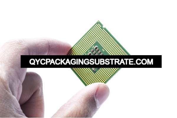
FCBGA package
Overall, FCBGA has successfully integrated into the field of IC packaging through its unique design and performance advantages, and occupies an important position in the evolution of chip packaging technology. In the process of continuously promoting the performance improvement of electronic equipment, FCBGA will undoubtedly continue to play a key role and provide more possibilities for future innovation.
What is the difference between FCBGA and PCB?
In the contemporary electronic landscape, the FCBGA (Flip-Chip Ball Grid Array) and PCB (Printed Circuit Board) stand out as crucial components in electronic devices. While they share some similarities, distinct differences set them apart. This article delves into a comprehensive exploration of these variances, zooming in on disparities between PWBs and PCBs, scrutinizing motherboards, substrates, and distinguishing between Substrate-like PCB (SLP) and HDI Substrate. By doing so, the aim is to provide readers with a nuanced understanding of the distinct roles these elements play in circuit packaging.
The basic difference between FCBGA and PCB
Although both FCBGA and PCB involve circuit packaging, there are significant differences in their basic design and purpose. FCBGA is mainly an integrated circuit packaging technology that uses a solder ball array to achieve electrical connections by flipping the chip directly and connecting it to the substrate. In contrast, PCB is a broader concept that refers to a printed circuit board, which contains a variety of components and connections.
The difference between PWBs and PCBs
PWBs (Printed Wiring Boards) are a type of PCBs. The main difference between them is that PWBs emphasize wider wiring and connections. FCBGAs are often directly connected to PWBs to form a compact package structure, thereby improving the performance and reliability of the circuit.
In electronic devices, the motherboard is the core of the device and is responsible for connecting various components, including the processor, memory, and expansion slots. The baseboard is part of the motherboard and is used to support and connect various components. FCBGA is usually installed directly on the motherboard and works together with other components to form a highly integrated system.
Substrate-like PCB (SLP) and High-Density Interconnect Substrate (HDI Substrate) are two variants of PCB. How are they related to FCBGA? SLP uses an integrated packaging method similar to FCBGA, making the PCB more compact and high-performance. HDI Substrate uses high-density interconnection technology to achieve more levels of wiring, improving the performance and signal transmission speed of the circuit board.
Despite these differences, FCBGA and PCB often work together. FCBGA improves the performance of the circuit through its highly integrated features, while PCB, as the backplane, provides support and connections for various components. This synergy enables electronic devices to achieve high performance and reliability more efficiently.
By in-depth understanding of the differences between FCBGA and PCB, we can better understand their unique roles in the electronics field. The mutual cooperation of the two promotes the continuous development of modern electronic equipment, providing more advanced and reliable technical support for our daily life and industrial applications.
What are the main structures and production technologies of FCBGA?
FCBGA (Flip-Chip Ball Grid Array), as a key integrated circuit packaging technology, shows unique characteristics in its main structure and production technology. Let’s take a closer look at this technology to better understand its importance in modern electronics.
What is the main structure of FCBGA? It uses an advanced packaging form that flips the chip over and connects it to a substrate, using an array of solder balls to make electrical connections. This flipped chip design allows more input/output pins to be accommodated in a limited space, improving device density and performance.
Production Technology: Improved HDI Manufacturing Technology
In the manufacturing process of FCBGA, improved HDI (High-Density Interconnect) manufacturing technology is adopted. This technology focuses on achieving higher connection density in a limited space. By using fine lines and smaller apertures, it effectively reduces the distance between components and improves signal transmission efficiency.
Improved HDI manufacturing technology maximizes the available surface of the circuit board for signal transmission channels through multi-layer stacking design. This not only improves the performance of the board, but also reduces the overall size of the system, making FCBGA ideal for high-performance applications.
Production technology: improved semi-additive method
Another key production technology in FCBGA manufacturing is the improved semi-additive method. This method effectively reduces waste and costs in the manufacturing process by adding necessary conductor materials to the surface of the substrate instead of the traditional full additive method.
The enhanced semi-additive method offers increased flexibility in the manufacturing process, allowing for adjustments based on specific design requirements. This not only enhances manufacturing efficiency but also diminishes the demand for raw materials, contributing to environmental friendliness.
FAQs of FCBGA
What is unique about FCBGA compared with other packaging technologies?
FCBGA (Flip-Chip Ball Grid Array) packaging technology has unique features compared with traditional packaging. First, its flip-chip design allows for more input/output pins, improving the chip’s performance. Secondly, the layout of the solder ball array makes the signal transmission path shorter, effectively reducing the signal transmission delay. This makes FCBGA ideal for high-performance applications.
What are the different types of FCBGA and what scenarios are they suitable for?
There are many different types of FCBGA, such as different ball grid array arrangements and solder ball arrangement densities. The choice of these types should be based on the specific application scenario. For example, for applications requiring higher density, a type with a tighter arrangement of solder balls may be selected.
What is the relationship between FCBGA and PCB?
Although FCBGA has similarities with PCB (Printed Circuit Board), there are some key differences between them. FCBGA is a packaging technology, and PCB is the basis for connecting and supporting various components in electronic devices. When designing a circuit board, you need to consider how the FCBGA packaged chip works with the PCB to ensure a stable and reliable connection.
What advanced technologies are used in the manufacturing process of FCBGA?
The manufacturing process of FCBGA adopts a series of advanced technologies, including improved HDI manufacturing technology and improved semi-additive method. The application of these technologies makes the packaging process more precise and improves the reliability and performance of FCBGA.
In what fields is FCBGA widely used?
FCBGA (Flip-Chip Ball Grid Array) packaging technology enjoys widespread utilization across diverse fields owing to its exceptional performance and reliability. Particularly prominent in applications demanding extensive data processing and high-speed signal transmission, such as communication equipment, computer servers, and high-performance computing, FCBGA technology stands as a preferred choice. Its deployment underscores a commitment to achieving superior functionality and dependable operation in scenarios where large data volumes and rapid signal transmission are critical requirements.
What is the future development trend of FCBGA?
With the continuous advancement of technology, FCBGA packaging technology is still evolving. Future development trends may include higher integration, smaller package sizes, and more advanced heat dissipation designs to meet the growing performance demands of electronic devices.
By in-depth understanding of these common issues, we can more fully understand the importance of FCBGA packaging technology in the electronic field and provide better support for future applications.