 Professional Flip-Chip Packaging Substrate Supplier

Ultra-small bump pitch substrate manufacture, we mainly produce ultra-small bump pitch substrate, ultra-small trace and spacing packaging substrate and HDI PCBs.
Packaging substrates, serving as the cornerstone of modern electronics, hold a position of paramount importance. Their significance extends beyond merely providing support and interconnections for various electronic components; it also encompasses a profound impact on the performance, stability, and reliability of electronic equipment. Typically concealed within electronic devices, packaging substrates bear the responsibility of housing chips, circuits, and other critical components, all while facilitating electrical connections and ensuring isolation to uphold the device’s proper operation. At the heart of this importance lies the dielectric material employed in packaging substrates.
This article delves deeply into dielectric materials, integral components of packaging substrates, with a keen emphasis on their characteristics and physical properties. It underscores the pivotal role these materials play in packaging substrate technology and emphasizes the criticality of comprehending their properties and the selection of suitable materials to guarantee the performance and reliability of electronic devices.
Most importantly, we will peer into the future, examining the evolving trends in dielectric materials technology to drive innovation and sustainable development in the realm of electronics.
By gaining a deeper understanding of packaging substrate dielectric materials, we can fathom their pivotal role in electronic devices and recognize that ongoing research and innovation are essential for propelling the electronics field forward. Amidst a landscape rife with challenges and opportunities, the centrality of dielectric materials will persist, guiding the future of electronic technology.
What is the dielectric material of the packaging substrate?
Within the realm of packaging substrates, dielectric materials hold a unique position due to their defining attribute of high electrical resistivity.The inherent resistance of these materials renders them exceptionally well-suited for deployment as insulating layers in electronic packaging, serving the vital function of averting current leakage between electronic components.
Uncovering the critical role of dielectric materials in packaging substrates
Dielectric materials assume a critical role within packaging substrates, serving various indispensable functions. They are instrumental in creating insulating layers on packaging substrates, thereby segregating different circuits and electronic components, while also affording protection against interference and damage. This insulation stands as a fundamental prerequisite for the proper operation of electronic equipment, as it safeguards against signal interference, thus upholding circuit reliability and performance.
Furthermore, dielectric materials are deployed to regulate heat and temperature within electronic components. They often exhibit remarkable thermal insulation properties, rendering them invaluable in providing thermal control within electronic equipment. This facet is pivotal in preserving the requisite operating temperature of components, a key factor in ensuring the stability and reliability of electronic equipment.
In summary, the pivotal role of dielectric materials in packaging substrates encompasses insulation, isolation, thermal regulation, and protective functions, all converging to uphold the high performance and reliability of electronic devices. They constitute an integral component of packaging substrate design, providing a sturdy foundation for advancements and innovation within the field of electronics.
Key Properties of Dielectric Materials
The characteristics of dielectric materials are of utmost importance in the design and functioning of packaging substrates. These properties encompass the dielectric constant, dielectric loss, and coefficient of thermal expansion, all of which wield significant influence in safeguarding the reliability and optimizing the performance of the packaging substrate.
Dielectric constant
The dielectric constant, often denoted as ε (the Greek letter epsilon), gauges a material’s capacity to react to an electric field. It quantifies alterations in the speed of electromagnetic wave propagation within materials, and it holds particular significance in radio frequency (RF) applications. A higher dielectric constant corresponds to a slower propagation of electromagnetic waves, exerting a more pronounced influence on high-frequency signals. Consequently, materials characterized by a low dielectric constant are of paramount importance in high-frequency packaging substrates, as they facilitate rapid signal transmission and minimal signal loss.
Different packaging applications may require materials with different dielectric constants, so engineers need to carefully select them to meet specific needs. In wireless communications or high-speed data transmission, materials with low dielectric constant will provide better performance and ensure fast and accurate transmission of signals.
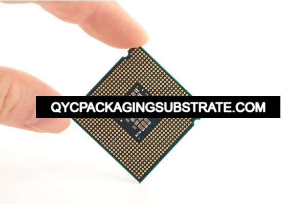
Ultra-small bump pitch substrate
Dielectric loss
In packaging substrates, dielectric loss is an important consideration because it directly affects signal transmission efficiency. High dielectric losses cause signal energy to be converted into heat, degrading package performance.
Reducing dielectric losses is key to improving package substrate performance. This can be achieved through the use of low-loss materials, optimized material handling processes and carefully designed structures. In high frequency and microwave applications, reducing losses is critical to ensuring signal quality.
Thermal expansion coefficient
The coefficient of thermal expansion, often expressed in ppm/°C (parts per million per degree Celsius), serves as a crucial metric measuring how a dielectric material expands or contracts in volume with temperature fluctuations. This property holds immense importance in preserving the stability of packaging substrates because temperature variations can lead to disparities in thermal expansion among different components, giving rise to stress and thermal-related concerns.
In situations where high temperatures prevail, aligning the thermal expansion coefficient of the packaging substrate material with that of other components becomes imperative. Opting for a material with a thermal expansion coefficient closely mirroring that of other materials can alleviate thermal stress, ensuring the stability and reliability of the packaging.
To sum up, essential dielectric material properties, encompassing the dielectric constant, dielectric loss, and coefficient of thermal expansion, assume a pivotal role in shaping the performance and reliability of packaging substrates. By judiciously selecting and optimizing these attributes, engineers can effectively address diverse packaging requirements, fostering high-performance and dependable packaging substrate designs.
Physical properties of packaging substrate dielectric materials
The performance and reliability of the packaging substrate hinge significantly on its physical properties. In this section, we delve deeper into the examination of two pivotal dielectric material characteristics: thermal conductivity and mechanical properties, elucidating their profound influence on the packaging substrate.
Thermal conductivity
Thermal conductivity represents a fundamental property of dielectric materials, serving as a determinant of their heat transfer capabilities. It quantifies a material’s capacity to efficiently transmit heat, commonly expressed as a thermal conductivity coefficient denoted in units of W/m·K. In the realm of packaging substrates, high thermal conductivity assumes paramount importance as it facilitates the efficient dissipation of heat and the maintenance of low-temperature operation within the device.
Given that various dielectric materials exhibit distinct thermal conductivities, the selection of an appropriate material becomes a critical consideration in meeting the specific thermal dissipation requirements of an application. Materials boasting high thermal conductivity can swiftly channel heat away from the packaged device to a heat sink or another cooling solution, ensuring that the device remains free from overheating even under substantial workloads.
Mechanical behavior
Packaging substrates require a certain amount of mechanical strength and stiffness to maintain their integrity under varying stress conditions. Mechanical properties include flexural strength, tensile strength and impact resistance, which are critical to the durability of the packaging substrate during installation, transportation and use.
A proper balance of strength and stiffness is critical to prevent micro-cracks or deformation of the package substrate due to environmental vibration or temperature changes. Proper mechanical properties can ensure the reliability of packaged devices under extreme conditions and extend their service life.
Furthermore, the packaging substrate’s ability to withstand unexpected physical shocks, such as drops or transportation-related jolts, adds another layer of critical consideration. This impact resistance is crucial to ensuring the durability and reliability of electronic devices.
In essence, the physical attributes of packaging substrates, encompassing factors like thermal conductivity and mechanical properties, wield a profound influence on the performance and dependability of electronic devices. By selecting the appropriate dielectric materials, specific thermal prerequisites and mechanical strength demands can be effectively addressed in diverse applications, thereby guaranteeing the proper functioning and prolonged service life of the device. In future research endeavors, we can anticipate the emergence of more innovative materials and designs aimed at further enhancing the performance and reliability of packaging substrates, aligning them with the evolving needs of the electronics industry.
Choose the right dielectric material
In the design of packaging substrates, selecting the appropriate dielectric material is critical. Here we provide some advice on how to select dielectric materials and highlight the importance of considering application requirements.
Understanding the role of permittivity and loss: First, engineers should have a deep understanding of the permittivity and loss characteristics of different dielectric materials. Materials with high dielectric constants generally provide better electrical properties, while lower losses reduce energy loss during signal transmission. Depending on the specific application, a balance between dielectric constant and losses is chosen.
Consider frequency range: Different applications involve different frequency ranges. Certain dielectric materials may perform well in high-frequency applications, while others are more suitable in the lower frequency range. Understand the frequency requirements of the application to select the most appropriate material.
Mechanical Properties: The mechanical requirements of the application are also considerations. Some materials may be more resistant to high temperatures, while others may perform better under mechanical stress. Comprehensive consideration of mechanical properties ensures materials can meet the needs of specific applications.
Emphasizes the importance of considering application requirements
Clearly Define Application Requirements: Before selecting a dielectric material, it is critical to clearly define the application requirements. This includes aspects such as frequency range, operating temperature, mechanical stress, etc. A clear definition of requirements helps in selecting suitable materials.
Work with a materials supplier: Work with a professional materials supplier who can often provide application-specific recommendations. Suppliers can provide important information on material performance, availability, and cost.
Consider Cost-Effectiveness: Cost is also a consideration when selecting dielectric materials. Performance needs should be weighed against available budget to ensure that the material selected strikes a balance between economic feasibility and performance.
Conduct real-world testing: Finally, verify that the selected material meets the application requirements through real-world testing and prototype verification. This helps identify potential issues and provides feedback to further optimize the design.
In a nutshell, the choice of the right dielectric material stands as a critical determinant in the performance and dependability of the packaging substrate. Engineers should strive to cultivate a comprehensive grasp of the characteristics inherent to various materials, precisely delineate application prerequisites, and actively engage with suppliers to guarantee the fulfillment of application-specific criteria, thereby attaining an optimum balance between performance and cost-effectiveness.
Future outlook
The field of packaging substrates is constantly evolving, and dielectric materials technology is also advancing with the times. In the future, we can expect the following important technology trends:
The surge in high-frequency applications, driven by the emergence of technologies like 5G and other advanced communication systems, will lead to a growing need for dielectric materials. Consequently, the research and development of dielectric materials tailored for high-frequency packaging will assume a pivotal role, representing a significant and crucial direction for innovation.
Lower losses: In the high-frequency packaging and microwave fields, reducing the losses of dielectric materials will become a continued focus. The development of new materials and manufacturing methods will help reduce energy losses in signal transmission.
Multifunctional materials: Dielectric materials of the future may not only have electrical properties, but may also have other functions such as thermal management, EMI shielding and mechanical strength. This will drive innovation and reduce packaging complexity.
Eco-friendly materials: Sustainability has become a core concern in the electronics industry. Future dielectric materials will pay more attention to environmental protection to reduce adverse impacts on the environment.
The criticality of innovative and sustainable practices
Within the continually advancing domain of packaging substrates, both innovation and sustainable practices stand as imperative cornerstones. Innovation serves as the driving force propelling technology towards new horizons, while sustainability remains the linchpin in our efforts to meet present-day demands and chart a course for enduring solutions that can benefit generations to come.
By continually exploring new ideas and approaches, we can improve the performance, reliability and efficiency of packaging substrates.
At the same time, sustainable practices mean taking proactive steps in resource use, waste management and environmental protection. This includes adopting renewable energy sources, reducing waste generation and reducing carbon footprint. By adopting these practices during manufacturing and use, we can reduce our impact on the environment.
In short, the future packaging substrate field will be full of opportunities, but also accompanied by challenges. Only through innovation and sustainable practices can we continue to move forward and make important contributions to the future development of the electronics field.