 Professional Flip-Chip Packaging Substrate Supplier

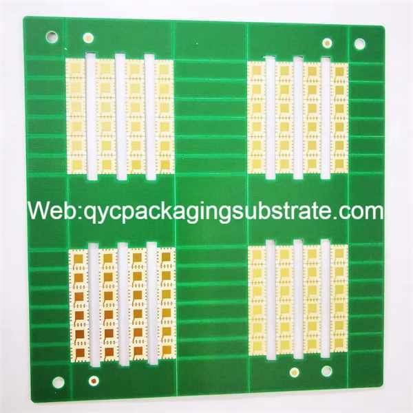
Ultra-small Spacing PCB
Ultra-small spacing PCB Vender. High Frequency Packaging Substrate manufacturing. we have used the Rogers materials to produce the High Frequency Packaging Substrate. the trace and spacin are 40/40um.
In the field of modern electronics, Package Substrate in Ultra-small Spacing High-Frequency PCB (Ultra-small Spacing High-Frequency PCB) is regarded as a crucial concept. This high-performance electronic component packaging technology carries chips and other key components, providing a solid foundation for the design of the entire circuit board. Let’s take a deeper look at Package Substrate’s key role in this space.
First of all, Package Substrate is not only a mechanical support for electronic components, but also the core to ensure the normal operation of chips and other components. Its exquisite structure can withstand the tiny spacing required for high-frequency electrical signal transmission, providing strong support for the performance of modern high-frequency communication equipment.
In circuit board design, Package Substrate plays a particularly significant role. Not only does it provide the necessary physical support, it also ensures that signals can be transmitted quickly and stably between components through its sophisticated electrical connections. This electrical connection involves not only basic signal transfer, but also precision processing of high-frequency signals to ensure optimal performance throughout the system.
In addition, Package Substrate is also responsible for isolating and protecting components in circuit board design. Through a cleverly designed structure, it can effectively isolate interference between different electronic components and ensure the stability and reliability of the system. This isolation effect is particularly important for ultra-fine pitch high-frequency PCBs, because high-frequency signals are often more susceptible to external interference.
On the whole, Package Substrate is an indispensable part of ultra-fine pitch high-frequency PCB. It plays a variety of functions in electronic equipment, from providing physical support to precision electrical connections to isolating and protecting components. Each aspect directly affects the performance of the entire system. Therefore, an in-depth understanding and rational application of Package Substrate is an important task for design engineers in the field of ultra-fine pitch high-frequency PCB, which provides a solid foundation for development and innovation in the electronic field.
Ultra-small spacing high frequency PCB
What are the functions of Ultra-small Spacing High-Frequency PCB?
In the field of modern electronics, one of the core components of Ultra-small Spacing High-Frequency PCB is Package Substrate. This key electronic component packaging structure is not only a provider of mechanical support, but also undertakes key electrical connection and signal transmission functions to ensure the normal operation of the entire electronic system.
First of all, as an infrastructure, Package Substrate’s mechanical support function is indispensable. In compact electronic devices, how to effectively support and secure chips and other key components is crucial to the stability of the entire system. Among them, the design requirements of ultra-fine pitch high-frequency PCBs are more demanding, and it is necessary to ensure that the Package Substrate can provide sufficient support in a limited space to prevent damage caused by mechanical vibration or external pressure.
However, Package Substrate’s capabilities are not limited to mechanical support. It also plays key electrical connection tasks in circuit design. Through precise circuit layout, Package Substrate provides reliable electrical connections for chips and other components, ensuring that signals can be efficiently transmitted between various parts. This is crucial for ultra-fine pitch high-frequency PCBs, because the transmission of high-frequency signals puts higher requirements on the stability and performance of the circuit.
On the other hand, Package Substrate’s function in signal transmission is even more eye-catching. Through precise wiring and design, it not only makes signal transmission between electronic components faster and more reliable, but also reduces interference between signals. In high-frequency PCBs, stable transmission of signals is crucial to the overall performance of the device, and Package Substrate plays a key role in this regard.
More importantly, how does Package Substrate ensure the normal operation of electronic components. By providing reliable mechanical support, excellent electrical connections and efficient signal transmission, Package Substrate plays a role in ensuring performance and stability in the entire system. It ensures that electronic components can operate normally at the high frequency required by the design by reducing the effects of circuit resistance, inductance and signal propagation delay.
In general, the Package Substrate in Ultra-small Spacing High-Frequency PCB is not just a simple support structure, but a complex and critical component that provides high performance and stability for modern electronic equipment through its multiple functions. Provides a solid foundation.
What are the different types of Ultra-small Spacing High-Frequency PCB?
In today’s electronic field, different types of Package Substrate are crucial to the design and application of ultra-fine pitch high-frequency PCBs. We will delve into the types of Rigid Substrate, Flex Substrate and Rigid-Flex Substrate to understand what scenarios they are suitable for, as well as their respective advantages and application areas.
First of all, Rigid Substrate (rigid substrate) is a common type of Package Substrate. Its main feature is its high mechanical strength and stability. This type of Package Substrate is usually used in scenarios that require high mechanical performance and relatively fixed size. For example, in electronic equipment that needs to support large chips and components, Rigid Substrate can provide sufficient mechanical support to ensure the overall stability of the system. Its advantage lies in its support for physical forms and is suitable for relatively static environments.
Secondly, Flex Substrate is known for its excellent flexibility and bending properties. This type of Package Substrate is useful in some special application scenarios, such as curved or bent devices. Flex Substrate can easily adapt to complex shapes and surfaces, so it is widely used in fields such as bending and wearable devices. Its flexibility makes it ideal for equipment with limited space or where a curved design is required.
Finally, Rigid-Flex Substrate is a Package Substrate that combines rigid and flexible properties. This type can combine the advantages of Rigid Substrate and Flex Substrate in one design, combining strength and flexibility. Rigid-Flex Substrate is often used in scenarios that require both stability and bending requirements, such as foldable smartphones or portable medical devices. It is designed to allow for rigid support of hardware elements while also being able to accommodate curved use of the device.
In general, different types of Package Substrate are suitable for various application scenarios and fully meet the requirements for mechanical performance and morphological flexibility in electronic device design. Design engineers need to fully consider the specific requirements of the device when selecting a suitable Package Substrate to ensure optimal performance in actual applications. This is also the key to understanding and selecting the appropriate type of Package Substrate in ultra-fine pitch high-frequency PCB design.
What is the relationship between Ultra-small Spacing High-Frequency PCB and IC packaging?
In the field of modern electronics, IC (integrated circuit) packaging is one of the key steps to realize the functionality of electronic devices. In this process, the combination of different packaging technologies such as BGA (Ball Grid Array) and QFP (Quad Flat Package) with Package Substrate has a profound impact on the performance and stability of the entire electronic product.
First of all, BGA is a common packaging technology that is characterized by tiny solder balls on the bottom of the chip. These solder balls form a solid electrical connection by melting and connecting to the corresponding pads on the Package Substrate. Due to the design of BGA, more pins can be implemented in a relatively small space, providing higher connection density. This compact design is particularly important for ultra-fine pitch high-frequency PCB applications because it allows more electronic components to be integrated into a small package, thereby improving overall system performance.
QFP, on the other hand, is a traditional flat package technology that has four flat pin arrangements around the package. Unlike BGA, the pins of QFP are directly connected to the Package Substrate through surface soldering. This form of packaging is typically used in applications that require lower pin count and connection density, but is still widely used in many electronic devices.
Package Substrate, as the basis of these packaging technologies, not only provides mechanical support, but also carries the key electrical connections between electronic components. Its superior high-frequency performance makes the signal transmission on the circuit board more reliable, which directly affects the performance of the entire electronic product. Especially for ultra-fine pitch high-frequency PCBs, the quality and performance of Package Substrate are particularly critical due to their design requirements for higher frequencies and shorter signal transmission paths.
In addition, the choice of packaging technologies such as BGA and QFP also directly affects the heat dissipation performance of electronic products. Due to its spherical bottom structure, BGA helps transfer heat more effectively and is suitable for scenarios with high heat dissipation requirements. The flat structure of QFP may require additional heat dissipation design.
To sum up, the integration of IC packaging technology and Package Substrate is a key link that cannot be ignored in electronic product design. Choosing the appropriate packaging technology, such as BGA or QFP, and ensuring its coordination with Package Substrate will directly determine the performance, reliability and heat dissipation effect of the entire system, laying a solid foundation for the application of ultra-fine pitch high-frequency PCBs.
How is Package Substrate different from traditional PCB?
The difference between Ultra-small Spacing High-Frequency PCB (ultra-small spacing high-frequency PCB) and traditional PCB appears in several key aspects, covering PWBs and PCBs, motherboards and various substrate types. These differences relate not only to structure and performance, but also to areas of application and possibilities for future development.
First of all, from the perspective of PWBs and PCBs, Ultra-small Spacing High-Frequency PCB focuses on smaller spacing and higher frequency. This requires more advanced materials and manufacturing processes to support higher-density component layout and faster signal transmission. In contrast, traditional PCBs pay more attention to versatility and stability, and may not need such compact requirements in the layout of components.
In terms of motherboard design, Ultra-small Spacing High-Frequency PCBs tend to focus more on specific application areas, such as high-speed communications or radio frequency applications. This means that the structure of the motherboard and the layout of components will be more precise to meet the needs of high-frequency signals. Traditional PCB motherboards are more for general purposes and have relatively low requirements for signal speed and frequency.
Regarding different types of substrates, Ultra-small Spacing High-Frequency PCB usually uses some advanced materials, such as low dielectric constant and low-loss high-frequency materials to ensure better performance in high-frequency environments. In comparison, traditional PCBs may use more general-performance substrate materials because they generally do not need to operate in the high-frequency range.
In addition, a special type among Ultra-small Spacing High-Frequency PCB is Substrate-like PCB (SLP). This design emphasizes ultra-thinness, lightness and high performance, and is suitable for scenarios where complex functions need to be implemented in a limited space. This is significantly different from the thickness and weight requirements of traditional PCBs.
Overall, Ultra-small Spacing High-Frequency PCB can better meet the needs of modern communications and radio frequency applications in high-frequency environments through innovations in design, materials and manufacturing processes. This is different from the design concepts and application scenarios of traditional PCBs, and represents an important progress in the field of electronic engineering in facing future technical challenges.
What are the main structures and manufacturing technologies of Ultra-small Spacing High-Frequency PCB?
In the field of ultra-fine pitch high-frequency PCB, the structure and manufacturing technology of Package Substrate are crucial topics. Let’s take a deeper look at how these key aspects shape the performance of this technology, especially when using advanced methods such as HDI (High-Density Interconnect) manufacturing technology and semi-additive methods.
Structure of Package Substrate
The structure of Package Substrate is designed to provide excellent performance and reliability in ultra-fine pitch high-frequency environments. Generally, it is composed of multiple layers of films, and the layers are connected through small through holes. This structure allows electronic components to be laid out in a compact space and to efficiently transmit signals.
With the application of HDI manufacturing technology, the structure of Package Substrate tends to be multi-layered and high-density. This structural design allows for more signal and power planes, improving the board’s signal integrity and interference immunity. At the same time, the ultra-thin insulation layer and fine through holes also help reduce the electrical distance between components, further improving performance.
The evolution of manufacturing technology: HDI manufacturing technology
HDI manufacturing technology is a key innovation in the field of Package Substrate. By using more precise processes, HDI technology can achieve higher circuit density and smaller spacing, thereby meeting the needs of ultra-fine pitch high-frequency PCBs.
FCBGA (Flip-Chip Ball Grid Array) packaging technology enjoys widespread utilization across diverse fields owing to its exceptional performance and reliability. Particularly prominent in applications demanding extensive data processing and high-speed signal transmission, such as communication equipment, computer servers, and high-performance computing, FCBGA technology stands as a preferred choice. Its deployment underscores a commitment to achieving superior functionality and dependable operation in scenarios where large data volumes and rapid signal transmission are critical requirements.
Evolution of manufacturing technology: semi-additive approach
The semi-additive method is another widely used technology in Package Substrate manufacturing. Compared with the traditional additive method, the semi-additive method adds conductive materials to some areas to reduce the electrical distance and improve signal transmission efficiency.
Through the semi-additive method, manufacturers can more accurately control the conductive path on the PCB, thereby optimizing the signal transmission path and reducing signal transmission loss. The introduction of this technology not only improves the performance of ultra-fine pitch high-frequency PCBs, but also helps reduce power consumption and extend the service life of electronic equipment.
In general, the evolution of Package Substrate in structure and manufacturing technology, especially the application of HDI manufacturing technology and semi-additive methods, provides more advanced and higher-performance solutions for ultra-fine pitch high-frequency PCBs. These innovations not only meet the performance and compact design needs of modern electronic devices, but also lay a solid foundation for future technological development.
Ultra-small Spacing High-Frequency PCB FAQs
What is the difference between ultra-fine pitch high-frequency PCB and traditional PCB?
Readers may be curious, in what aspects are there significant differences between Ultra-small Spacing High-Frequency PCB and traditional PCB? How does this difference affect performance and application areas? What are the technical differences between the keyword “Ultra-small Spacing High-Frequency PCB” and “Traditional PCB”?
What is the role of Package Substrate in electronic devices?
What is the exact role of Package Substrate in electronic devices? Not only does it provide mechanical support, but how does it also support the electrical connections of critical components? How does this relate to Ultra-small Spacing High-Frequency PCB technology?
How to choose the appropriate Package Substrate type?
What are the key factors to consider when choosing a Package Substrate type? How will the specific application scenarios of Ultra-small Spacing High-Frequency PCB affect this selection process?
What are the common Ultra-small Spacing High-Frequency PCB application areas?
In what fields is Ultra-small Spacing High-Frequency PCB technology widely used? How does it meet the needs of different industries for high frequency and small spacing?
What are the innovations in Package Substrate’s manufacturing technology?
What are the innovations in Package Substrate’s manufacturing technology? How do these innovations improve the performance and reliability of Ultra-small Spacing High-Frequency PCBs?
What is the future development trend of ultra-fine pitch high-frequency PCB technology?
Readers may be concerned about the future development direction of Ultra-small Spacing High-Frequency PCB technology. What are the exciting trends in innovation and application in this technology field?
By answering these questions, we hope readers will gain a more comprehensive understanding of Ultra-small Spacing High-Frequency PCB technology and thus better apply it in their actual projects.