 Professional Flip-Chip Packaging Substrate Supplier

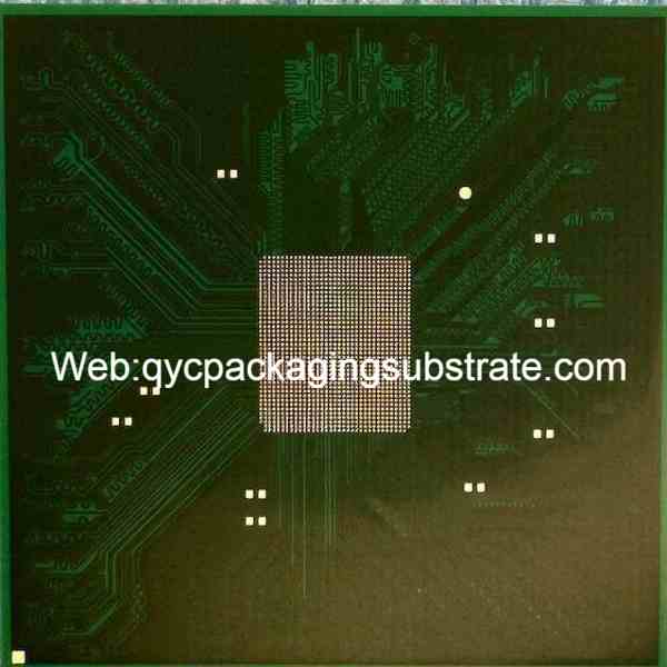
Professional Flip-Chip Package Substrate manufacturing, ultra-small pitch Bump is 100um, ultra-small trace and pitch 10um/10um, high frequency and high speed material packaging substrates.
Flip Chip Package Substrate is a key semiconductor packaging technology that plays an important role in the electronics industry. This article will introduce you to the key concepts, manufacturing processes, application areas, advantages and design considerations of Flip Chip Package Substrate.
Introduction to the packaging substrate
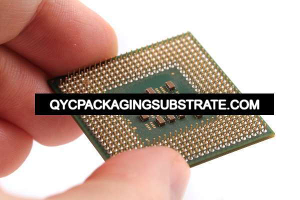
Flip Chip Package Substrate is an advanced packaging technology in which semiconductor chips are connected to a substrate upside down, achieving high-density interconnection through tiny solder joints. This method improves signal transmission speed and performance by shortening the electrical connection distance. The backside of the chip is connected to metal pads on the substrate via microspheres or other connections instead of traditional chip wire connections. This packaging method helps improve integration, reduce device size, improve reliability, and is suitable for a variety of applications.
Flip-Chip Package Substrate Manufacturing process
The manufacturing process of Flip Chip Package Substrate includes several key steps. First, a suitable substrate material is selected, typically silicon, glass, organic substrates, or ceramics. Then, circuits and interconnections are built on the substrate, the chip is mounted, and the chip pins are connected to the substrate through soldering. Encapsulation materials are used to protect the chip, while thermal structures help manage the heat generated. Finally, testing and inspection are conducted to ensure product quality.
Application fields
Flip Chip Package Substrate is widely used in various application fields, including computers, communication equipment, automotive electronics, medical electronics, consumer electronics and industrial automation. It provides superior solutions in terms of high performance, high density interconnection, high frequency performance and compact design.
Advantages
The advantages of Flip Chip Package Substrate include high-density interconnection, compact design, high-frequency performance, excellent thermal performance and multi-layer design. This helps improve device performance, reduce size, and improve reliability.
Design considerations
When designing Flip Chip Package Substrate, factors such as chip layout, thermal management, material selection, interconnect design, soldering technology, signal integrity and repairability need to be considered. Proper design can improve product performance and reliability.
In short, Flip Chip Package Substrate technology represents the future of semiconductor packaging, providing advanced solutions for various applications. Its high performance and versatility make it popular in the electronics industry, supporting innovation and growth.
We focus on manufacturing 10 to 18 layers of fine pitch Flip Chip Packaging Substrate. Our optimal line width and space are 9 micron/9 micron, providing customers with superior performance. Most customers’ line width and line spacing are approximately 20 micron/20 micron, but we can provide flexible multi-layer drilling options for 18-layer packaging substrates upon request. Regardless of a client’s specific requirements, we are committed to providing high quality, highly customizable solutions. Our team looks forward to working with you to meet your packaging substrate needs.
Flip-Chip Package Substrate
What is flip chip Package substrate Process
The Flip Chip Package Substrate process is an advanced semiconductor packaging technology that provides high-performance, high-density interconnection and reliability solutions for electronic devices. The following is a detailed introduction to the process of flipping the chip packaging substrate.
Flip chip Package substrate Material selection and preparation
The first step in the process involves selecting an appropriate substrate material, which typically includes silicon, glass, organic substrates, or ceramics. The choice of substrate material depends on application needs such as thermal conductivity, mechanical strength and dimensional requirements.
Circuit and interconnection design
After selecting the substrate material, the circuit and interconnection lines are designed. This includes determining chip layout, pad placement, interconnect line width and spacing, etc. The quality of interconnect design is critical to process success, affecting the quality and reliability of signal transmission.
Chip installation
After the interconnection design is completed, the semiconductor chip is mounted to the substrate. This usually involves connecting the backside of the chip to metal pads on the substrate. These connections can be microball soldering, soldering, or other connections, depending on the specific needs.
Welding
Soldering is a critical step in the manufacturing process, ensuring that the chip pins are securely connected to the connection points on the substrate. The soldering material is heated, melted, and then cooled to form a strong connection. This ensures high density interconnection.
Heat dissipation design
Flipping chip packaging substrates often requires efficient thermal design to manage the heat generated. This may include heat sinks, thermal pads, thermal vias, etc. to ensure that the chip does not overheat during operation.
Packaging materials
To protect the chip and provide mechanical stability, encapsulation materials are often added. These materials can be resins, plastics or other compounds used to cover and protect the chip and its connections.
Testing and Inspection
Finally, testing and inspection are performed to ensure the success of the process. This includes electrical performance testing, welding quality inspection, visual inspection and verification of other key parameters. Any defects or issues need to be fixed promptly.
How is Flip-Chip Package substrate manufactured?
The manufacturing of Flip-Chip Package Substrate is a complex project designed to achieve high-density interconnection and reliability. Below is a detailed introduction to the manufacturing process.
Substrate material selection
The first step in the process involves selecting an appropriate substrate material. Typically, you can choose silicon, glass, organic substrates (such as BGA substrates) or ceramics. Material selection depends on the requirements of the application, including thermal conductivity, mechanical strength and size.
Circuit design and preparation
After the substrate material is determined, the circuit and interconnection lines are designed, which includes determining the chip layout, pad layout, interconnection line width and spacing, etc. The key goal of this design phase is to ensure that the circuit can be connected effectively and meet performance requirements.
Chip installation
Next, the semiconductor chip is mounted on the substrate. This is usually done by connecting the backside of the chip to metal pads on the substrate. These connections are typically solder ball bonding, solder bonding, or other connections, depending on the process and application requirements.
Welding
Flip-Chip Package Substrate Soldering is a critical step in the manufacturing process that connects the chip’s pins (or solder balls) to the metal pads on the substrate. This soldering technique is often called ball grid array (BGA) soldering because the tiny solder balls are arranged in an array.
Heat dissipation design
The heat dissipation design of the flip-chip package substrate (Flip-Chip Package Substrate) is crucial. By optimizing the heat dissipation design, heat is effectively dispersed, the chip temperature is kept stable, and device performance and life are improved. This includes the use of thermally conductive materials, heat sinks, fans and other technologies to ensure the reliability of the chip in high power and high temperature environments.
Packaging materials
The packaging materials of Flip-Chip Package Substrate usually include substrate materials (such as silicon, glass, organic substrates, etc.), packaging materials (used to protect chips and connections), and soldering materials (solder balls or other connection methods) s material). These materials play a key role in the packaging process, ensuring reliable connections and superior device performance.
Testing and Inspection
Flip-Chip Package Substrate testing is an important step to ensure product quality. Testing typically includes visual inspection, electrical testing, solder joint integrity testing, interconnect testing and thermal performance testing. These tests ensure that the package substrate meets specifications, is defect-free, and operates reliably under a variety of environmental conditions.
Summarize
The fabrication of flipped chip packaging substrates is a highly sophisticated process that combines multiple critical steps to produce high-performance semiconductor packaging substrates. This manufacturing process has been widely used in computers, communications, automotive, medical and other fields to provide smaller and more powerful solutions for electronic devices. Through continuous improvement and optimization, the manufacturing process of flipped chip packaging substrates will continue to drive innovation and development in the electronics field.
Package substrate Application areas
Packaging substrate is a vital electronic component that is widely used in many fields and provides critical support and performance enhancement for various electronic devices. The following is a detailed introduction to the application areas of packaging substrates:
Computers and data centers: Packaging substrates play an important role in computer hardware, connecting and supporting central processing units (CPUs), memory, storage devices and other key components. They help improve computer performance and reliability.
Communication equipment: Whether it is smartphones, network equipment or satellite communication systems, packaging substrates provide key support for the high-frequency transmission of communication equipment. They allow high-speed data transfer and reliable communication connections.
Automotive electronics: Modern automobiles include many electronic control units (ECUs), and packaging substrates are used to connect and support these ECUs, including engine control units, safety systems, and entertainment systems.
Medical electronics: Medical devices, such as X-ray machines, pacemakers and medical imaging equipment, rely on packaging substrates to ensure reliable performance and data processing.
Consumer electronics: Consumer electronics such as smartphones, tablets, TVs, and audio systems use packaging substrates to support high performance and compact designs.
Industrial automation: Package substrates are used to control and monitor industrial automation equipment, such as robots, sensors and PLCs. They ensure reliable operation of the device and data processing.
Aerospace: In the aerospace field, packaging substrates are used in satellites, navigation equipment, aircraft control systems, etc. to ensure reliability and performance under extreme conditions.
Military applications: Packaging substrates are used in the military field for radars, communication equipment, missile systems and tactical control equipment. They must provide outstanding performance in demanding environments.
In summary, packaging substrates play a key role in various fields, supporting the high performance, high reliability and compact design of modern electronic devices. As technology continues to evolve, packaging substrates will continue to play an increasingly important role in various fields, driving innovation and improving the performance of electronic devices.
Flip-Chip Package Substrate
Commonly used packaging substrates Material
Flip-Chip Package Substrate uses many different types of substrate materials. The specific choice depends on application needs, performance requirements and cost considerations. The following are some commonly used packaging substrate materials:
Silicon: Silicon is a common substrate material with good mechanical strength and thermal conductivity. It is typically used in high-performance and high-density interconnect applications such as microprocessors.
Glass: Glass substrate is commonly used in optoelectronic applications such as image sensors and displays. It has good transparency and is suitable for optical and sensor devices.
Organic Substrates: Organic substrates include FR-4, BGA substrates, etc., which are usually used in communication equipment, consumer electronics and general packaging applications. They are relatively cheap and easy to process, but may be limited in high-frequency applications.
Ceramic: Ceramic substrates have excellent thermal conductivity and mechanical strength and are usually used in high-frequency radio frequency applications, microwave devices and applications in high-temperature environments.
RF Substrates: Substrate materials specially designed for RF and microwave applications, such as PTFE (polytetrafluoroethylene) and RO4350B. They have low dielectric constant and low loss, making them suitable for high-frequency communication equipment.
Composite Materials: Composite material substrates are usually made from a combination of different materials to take into account various performance requirements. They can be used in different areas, choosing the appropriate material combination according to needs.
Copper Substrates: Copper substrates are usually used in high-power electronic equipment and have good heat dissipation properties. They are suitable for power amplifiers and other high power applications.
Nickel Substrates: Nickel substrates are used in some special applications, such as electronic equipment in high-temperature environments, because nickel has good high-temperature stability.
We have a wide variety of Flip Chip Packaging Substrate materials, including Showa Denko brand base materials such as MCL-E-705G, MCL-E-770G, MECL-E-700G, MECL-E-795G, and more. Additionally, we offer Ajinonoto brand base materials, including GX92R, GXT31R2, GZ41R2H, GL102R8HF, GL103R8H, and others. Most of these base materials are suitable for high multilayer packaging substrates.Regarding soldermask layers, we have different types like SR7300G, PSR-4000 AUS703, PSR-800 AUS SR1.We also provide various surface finishing options, including ENEPIG, IT, ENEPIG+SOP, IT+SOP, Thin Ni ENEPIG, among others.If you have any questions, please feel free to contact us. It would be our honor to assist you, and we will respond as soon as possible.
Different packaging substrate materials are suitable for different application areas, so their performance and cost need to be considered based on specific needs when selecting. The material selection of the packaging substrate has an important impact on the performance and reliability of the entire electronic product.
What is flip chip packaging?
Flip-Chip Package Substrate is an advanced semiconductor packaging technology that has played an important role in the electronics industry. It provides outstanding performance, high-density interconnection, compact design and reliability by changing the way semiconductor chips are connected to packaging substrates. This article will provide an in-depth discussion of the working principle, manufacturing process, application areas, advantages and future development trends of flipped chip packaging substrates.
Working principle
The core principle of flipping the chip packaging substrate is to change the way the chip is connected. Traditional packaging technology typically uses wire bonding to connect the chip pins to the package substrate, while flip chip packaging uses tiny solder balls or other connections to connect the backside of the chip (chip chip) to metal pads on the substrate. . This approach shortens circuit paths, improves performance, and provides higher density interconnects. Flipping the chip package also helps improve thermal performance, making it particularly suitable for high-power and high-frequency applications.
Manufacturing process
The manufacturing process for flipping chip packaging substrates involves multiple steps. First, an appropriate substrate material is selected, typically silicon, glass, organic substrates, or ceramics. Then, circuits and interconnections are built on the substrate to determine the chip layout. Next, the chip is mounted to the substrate, and soldering is used to connect the chip pins to the connection points on the substrate. Soldering usually uses tiny solder balls or other connection methods to ensure a tight connection. Finally, encapsulation materials are used to protect the chips and connections and ensure the stability of electronic components.
Application areas
Flip chip packaging substrates have been widely used in multiple application areas, including but not limited to:
Computers and Servers: Used in high-performance processor and memory packages.
Communication equipment: supports high-speed data transmission and radio frequency applications.
Automotive electronics: used in engine controls, safety systems and entertainment systems.
Medical Electronics: Provides high performance in medical imaging and diagnostic equipment.
Consumer Electronics: Used in products such as smartphones, tablets, and televisions.
Industrial automation: Supports equipment such as robots, sensors, and PLCs.
Aerospace: used in satellites, navigation equipment and aircraft control systems.
Military Applications: Provides reliability and performance in radar, communications equipment and missile systems.
What is the main advantage of a flip chip package?
Flip-Chip Package Substrate, as an advanced semiconductor packaging technology, has many advantages, which make it popular in many application fields. The following are the main advantages of flip chip packaging:
High-density interconnection: Flip the chip packaging substrate to use tiny solder balls or other connection methods to connect the back of the chip to metal pads on the substrate, thereby achieving high-density interconnection. This helps reduce circuit paths, lower circuit latency, and improve performance.
Compact design: Since flip chip packaging allows the chip to be directly connected to the substrate without the need for leads, a more compact package design can be achieved. This is very important for miniaturized equipment and applications in tight spaces.
High frequency performance: Flip chip packaging has excellent high frequency performance and is suitable for radio frequency (RF) applications and high-speed data transmission. Its low inductance and capacitance properties allow it to perform well at high frequencies.
Excellent heat dissipation performance: Since the chip is directly connected to the substrate, flipping the chip package contributes to effective heat dissipation. This is critical for high-power applications and electronic devices in high-temperature environments.
Multi-layer design: Flip chip packaging supports multi-layer interconnections, which means more circuit layers can be implemented within the same package. This helps increase circuit complexity and reduce device size while providing more functionality.
Reliability: The connection method of flip chip packaging is usually more stable and reliable, reducing the risk of lead breakage or desoldering, and increasing the life of the device.
Suitable for a variety of application fields: Flip chip packaging is suitable for many fields such as computers, communication equipment, automotive electronics, medical equipment, consumer electronics, industrial automation, and aerospace. Its flexibility and broad applicability make it the packaging technology of choice for a variety of applications.
In summary, the advantages of flipping chip packaging substrates make it an indispensable packaging technology in the electronics industry. As technology continues to evolve, it will continue to provide critical support for the performance and reliability of electronic devices and drive innovation in various application areas.
Summarize
Flip-Chip Package Substrate represents a major innovation in the field of electronic packaging. This technology provides high-density interconnection, compact design and superior performance by connecting the backside of the semiconductor chip directly to the substrate. It is suitable for many application fields, including computers, communication equipment, automotive electronics, medical electronics and industrial automation. The flip-chip package provides excellent high-frequency performance for high-speed data transmission and RF applications, while providing excellent thermal performance for high-power devices.
The manufacturing process includes substrate selection, circuit design, chip mounting, connection method selection, welding and packaging to ensure strong and reliable connections. Future trends in flipped chip packaging include higher density interconnects, smaller sizes, higher frequencies, lower power consumption and more complex thermal designs.
In summary, flip chip packaging substrate technology has changed the face of electronic packaging, delivering superior performance and reliability. It has broad application prospects in the electronics industry and will continue to provide critical support for the growing demand for electronic equipment.
FQAs
The following are some frequently asked questions and their answers related to Flip-Chip Package Substrate:
What is a flip chip packaging substrate?
Flip chip packaging substrate is a semiconductor packaging technology that uses tiny solder balls or other connections to connect the backside of the semiconductor chip to metal pads on the packaging substrate. This connection method features high-density interconnection, compact design and high performance.
What is the difference between flip chip packaging and traditional packaging technology?
Traditional packaging technology usually uses wire bonding to connect the chip pins to the substrate, while flip chip packaging uses backside connection, which reduces circuit paths and improves performance.
What application fields is flip chip packaging suitable for?
Flip chip packaging is widely used in many fields such as computers, communication equipment, automotive electronics, medical electronics, consumer electronics, industrial automation, aerospace and military applications.
What are the advantages of flip chip packaging?
It features high-density interconnection, compact design, high-frequency performance, excellent thermal performance, multi-layer design and reliability.
What are the materials used to make flip chip packaging substrates?
Materials for manufacturing flip chip packaging substrates include silicon, glass, organic substrates, ceramics, etc. The specific choice depends on the application requirements.
Is flip chip packaging suitable for high frequency RF applications?
Yes, flip-chip packaging is ideal for high-frequency RF applications because of its low inductance and capacitance characteristics, which enable high-frequency transmission.
What is the manufacturing process of flip chip packaging substrate?
The manufacturing process includes substrate selection, circuit design, chip mounting, connection method selection, soldering and packaging to ensure tight connections and protect the chip.
What is the future development trend of flip chip packaging?
Future development trends include higher density interconnections, smaller sizes, higher frequencies, lower power consumption and more complex heat dissipation designs to meet the growing demand for electronic devices.
Is flip chip packaging suitable for mass production?
Yes, flipped chip packaging is already widely used in mass production and is used to produce a variety of electronic devices.