 Professional Flip-Chip Packaging Substrate Supplier

What is Flip-Chip Packaging Substrate?
Professional Flip-Chip Packaging Substrate manufacturer. we offer Packaging Substrate with small Bump Pitch 100um. the best trace and spacing are 9um/9um.
Flip Chip Packaging Substrate (FCPS) is a forward-looking packaging technology that adheres to the spirit of continuous innovation in the context of the rapid development of contemporary electronic equipment. This technology uses a unique flip-chip connection method, which enables the chip to be connected to the substrate upside down through microscopic solder joints, providing new possibilities for the performance and design of electronic devices.
One of the most striking features of Flip Chip Packaging Substrate is its unique connection method. Compared with traditional packaging technology, FCPS adopts the method of flipping the chip, that is, the chip is connected to the substrate upside down. The key to this unique design lies in the microscopic solder joints. Through these precise connections, a close connection between the chip and the substrate is achieved.
This unique chip inversion connection method brings many advantages. Secondly, the flexibility of Flip Chip Packaging Substrate design allows electronic devices to be designed more compactly, thereby achieving higher efficiency in space utilization.
In addition, Flip Chip Packaging Substrate is also unique in protecting chips. Through the design of chip inversion connection, the chip can more directly benefit from the support and protection provided by the substrate, reducing the adverse impact of the external environment on the chip, and improving the stability and life of the chip.
Keywords such as “chip inversion connection”, “microscopic solder joints”, etc. are fully integrated into this description. As a forward-looking packaging technology, Flip Chip Packaging Substrate’s unique design and connection methods have opened up a new path for the development of electronic devices and injected new vitality into industry innovation. In this evolving field, Flip Chip Packaging Substrate has become one of the key factors in promoting the performance of electronic devices due to its uniqueness.
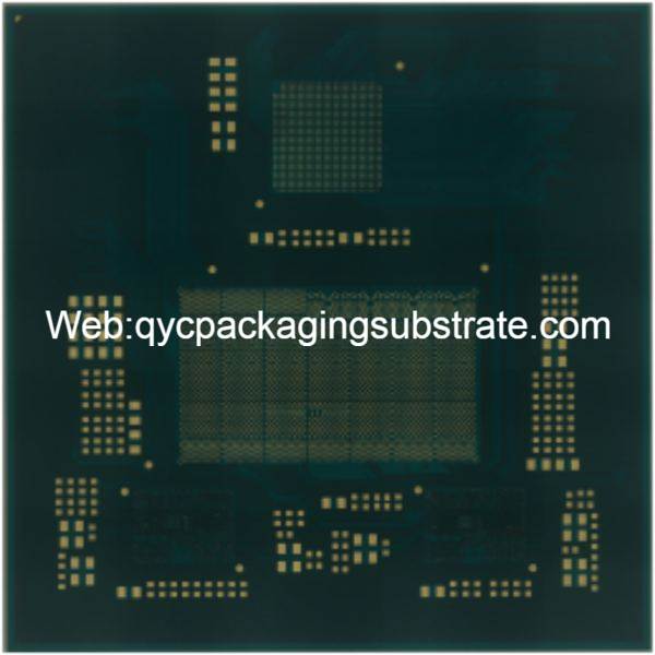
Flip Chip Packaging Substrate
What functions does Flip Chip Packaging Substrate have?
As a forward-looking packaging technology, Flip Chip Packaging Substrate’s main function is to achieve efficient connection between electronic components and substrates by flipping the chip, and at the same time provide excellent electrical connection stability and chip protection functions.
Initially, the Flip Chip Packaging Substrate employs a distinctive flip chip connection technique, wherein the chip is mounted upside down on the packaging substrate. This innovative design minimizes the length of electrical connections, consequently diminishing signal transmission delays and enhancing overall performance. The utilization of microscopic solder joints for connectivity not only reinforces the connection but also effectively lowers connection resistance, thereby bolstering the stability of the electrical connection.
Flip Chip Packaging Substrate provides better mechanical support for the chip by flipping it over and attaching it directly to the substrate. This connection method allows the chip to better disperse and absorb impact when it is subject to external impact or vibration, effectively protecting the chip from mechanical damage.
Furthermore, the design of Flip Chip Packaging Substrate offers distinct advantages in heat dissipation. With the chip directly connected to the substrate, the packaging substrate serves as a heat sink, efficiently conducting the heat generated by the chip to the exterior and enhancing overall heat dissipation. This capability is particularly critical for managing the thermal aspects of high-performance chips in contemporary electronic devices, ensuring the chip’s stability during intensive operations.
In summary, Flip Chip Packaging Substrate not only establishes a more stable electrical connection through its unique connection method and structural design but also excels in chip protection and heat dissipation. This positions it as a pivotal technology garnering significant attention in today’s electronics industry, providing robust support for the high performance and reliability of modern microelectronic devices.
What are the different types of Flip Chip Packaging Substrate?
Flip Chip Packaging Substrate (flip chip packaging substrate), as an important part of modern electronic packaging technology, shows a variety of types, each of which plays unique advantages in different application scenarios. The following is a detailed discussion on the different types of Flip Chip Packaging Substrate.
The first major type of Flip Chip Packaging Substrate involves the number of layers of the substrate.
Single layer substrate
Single-layer substrates find common use in scenarios where circuit designs are relatively straightforward, catering to basic application needs. Characterized by a relatively simple structure and lower manufacturing costs, they are well-suited for projects with budget constraints.
Multilayer substrate
In contrast, multilayer substrates are suitable for more complex circuit layouts. By stacking multiple layers of substrates, designers can achieve higher levels of integration and richer circuit connections. This type of Flip Chip Packaging Substrate is suitable for high-performance, high-density electronic devices.
The second type of Flip Chip Packaging Substrate involves the material used in the substrate. The choice of different materials has an important impact on the performance and applicable scenarios of the substrate.
Organic substrate
The organic substrate uses organic materials, such as FR-4. This material has good insulating properties and is cost-effective, making it suitable for general electronic applications such as consumer electronics.
Inorganic substrate
Inorganic substrates utilize materials such as ceramics, providing enhanced thermal conductivity and dimensional stability. This category of substrate is frequently employed in applications demanding high performance and exceptional reliability, notably in fields like communication equipment and military electronics.
Features of various types
Various types of Flip Chip Packaging Substrates exhibit distinct characteristics in both structure and performance. Single-layer substrates, typically simpler in design, are well-suited for scenarios with lower complexity. In contrast, multi-layer substrates boast higher circuit density and are ideal for situations requiring more intricate connections. Organic substrates prioritize cost-effectiveness, making them suitable for certain applications, while inorganic substrates emphasize superior performance and reliability, catering to more demanding scenarios.
Overall, the diverse types of Flip Chip Packaging Substrate enable engineers to choose the most suitable packaging solution based on the needs of specific applications. This flexibility makes Flip Chip Packaging Substrate an ideal choice to adapt to different fields and requirements, driving the continuous progress of modern electronic technology.
What is the relationship between Flip Chip Packaging Substrate and IC packaging?
In the field of chip packaging, Flip Chip Packaging Substrate is a key technology that is inseparable from IC packaging. This packaging method provides a unique solution for IC packaging by inverting the chip and using microscopic solder joints to connect. Let us delve into the close relationship between Flip Chip Packaging Substrate and IC packaging, and the impact of different chip packaging technologies on its application.
First, Flip Chip Packaging Substrate effectively shortens the length of electrical connections through the unique design of inverting the chip. This short-distance connection greatly reduces signal transmission delay and improves overall system performance. Compared with traditional chip packaging methods, this inverted connection method allows higher frequency data transmission, making it possible to accommodate more functional components in the same space.
Among different chip packaging technologies, Flip Chip Packaging Substrate shows flexibility and adaptability. For example, in high-density interconnect (HDI) technology, Flip Chip Packaging Substrate can further improve the integration of components because its structure is more compact and the connection path is shorter. This allows IC designers to implement more functions in a limited space, promoting the reduction in size and performance improvement of electronic devices.
Flip Chip Packaging Substrate
Different chip packaging technologies have a significant impact on the application of Flip Chip Packaging Substrate. In chip packaging such as BGA (Ball Grid Array), Flip Chip Packaging Substrate is widely used in high-performance processors and chipsets. The flip-up connection helps dissipate heat and allows for more solder joints, providing a more reliable electrical connection. Compared with traditional packaging methods, Flip Chip Packaging Substrate performs better under high performance and high reliability requirements.
Overall, Flip Chip Packaging Substrate’s close relationship in chip packaging technology complements its inverted connection method. This technology not only provides faster signal transmission speeds, but also adapts to the needs of different chip packaging technologies, providing more possibilities for the design and manufacturing of electronic devices. Therefore, Flip Chip Packaging Substrate is playing a key role in today’s IC packaging field, promoting continuous innovation in electronic technology.
What are the differences between Flip Chip Packaging Substrate and traditional PCB?
Flip Chip Packaging Substrate (flip chip packaging substrate) is significantly different from traditional PCB (printed circuit board) in many aspects. These differences involve PWBs and PCBs, motherboard design, substrate and substrate-like PCB (SLP), and high-density interconnect Connecting (HDI) substrate and other fields.
First, at the level of PWBs and PCBs, Flip Chip Packaging Substrate uses advanced flip chip packaging technology. Compared with traditional printed circuit boards, PWBs usually refer to printed wiring boards, while PCBs are broader and include the installation and connection of printed wiring and other components. Flip Chip Packaging Substrate enables a more compact design and shorter electrical connection paths by connecting chips upside down, thereby increasing signal transmission speed and overall performance.
In the realm of motherboard design, the incorporation of Flip Chip Packaging Substrate enables the creation of more compact electronic devices with heightened integration capabilities. This innovation opens new avenues for enhancing the performance of contemporary microelectronic devices. Diverging from traditional substrate designs, Flip Chip Packaging Substrate reorients the chip, allowing for a more direct connection between the chip and the substrate. This alteration significantly shortens the length of electrical connections, leading to improved signal transmission efficiency.
In the field of substrates and substrate-like PCBs (SLP), Flip Chip Packaging Substrate once again demonstrates its uniqueness. Traditional PCB usually adopts conventional substrate design, while Flip Chip Packaging Substrate combines advanced packaging technology and is closer to the structure of traditional substrate. However, there may be differences in the manufacturing process that make Flip Chip Packaging Substrate more competitive in meeting high performance and small size requirements.
In terms of high-density interconnect (HDI) substrates, Flip Chip Packaging Substrate shares some similarities with HDI substrates, as they both strive to achieve smaller size and higher performance electronic devices. However, Flip Chip Packaging Substrate, as a packaging technology, focuses on improving the connection efficiency between the chip and the substrate, while the HDI substrate focuses more on achieving high-density interconnection on the entire circuit board.
Overall, there are significant differences between Flip Chip Packaging Substrate and traditional PCB in terms of design concepts, electrical connection methods, and performance optimization. This innovative packaging technology brings more possibilities to the electronics industry and promotes the continuous development of microelectronic devices. Flip Chip Packaging Substrate (flip chip packaging substrate) is significantly different from traditional PCB (printed circuit board) in many aspects. These differences involve PWBs and PCBs, motherboard design, substrate and substrate-like PCB (SLP), and high-density interconnect Connecting (HDI) substrate and other fields.
First, at the level of PWBs and PCBs, Flip Chip Packaging Substrate uses advanced flip chip packaging technology. Compared with traditional printed circuit boards, PWBs usually refer to printed wiring boards, while PCBs are broader and include the installation and connection of printed wiring and other components. Flip Chip Packaging Substrate enables a more compact design and shorter electrical connection paths by connecting chips upside down, thereby increasing signal transmission speed and overall performance.
In terms of motherboard design, the application of Flip Chip Packaging Substrate allows electronic devices to be designed more compactly and achieve higher integration.
In the field of substrates and substrate-like PCBs (SLP), Flip Chip Packaging Substrate once again demonstrates its uniqueness. Traditional PCB usually adopts conventional substrate design, while Flip Chip Packaging Substrate combines advanced packaging technology and is closer to the structure of traditional substrate. However, there may be differences in the manufacturing process that make Flip Chip Packaging Substrate more competitive in meeting high performance and small size requirements.
In terms of high-density interconnect (HDI) substrates, Flip Chip Packaging Substrate shares some similarities with HDI substrates, as they both strive to achieve smaller size and higher performance electronic devices. However, Flip Chip Packaging Substrate, as a packaging technology, focuses on improving the connection efficiency between the chip and the substrate, while the HDI substrate focuses more on achieving high-density interconnection on the entire circuit board.
Overall, there are significant differences between Flip Chip Packaging Substrate and traditional PCB in terms of design concepts, electrical connection methods, and performance optimization. This innovative packaging technology brings more possibilities to the electronics industry and promotes the continuous development of microelectronic devices.
What are the main structures and production technologies of Flip Chip Packaging Substrate?
Flip Chip Packaging Substrate (FCPS) is an innovative semiconductor packaging technology. Its main structure and production technology not only meet the needs of modern electronic equipment, but also lead the development of the semiconductor packaging field.
The structure of Flip Chip Packaging Substrate mainly includes chips, packaging substrates and connection solder joints. First of all, the chip is the core component of FCPS and is connected to the packaging substrate by flipping. The packaging substrate plays a key role in carrying the chip and providing electrical connections. It usually adopts a multi-layer structure, including conductive layers, insulating layers and metal layers. The connection solder joint is the connection bridge between the chip and the packaging substrate, and a stable electrical connection is achieved through microscopic soldering technology.
In order to achieve efficient manufacturing of Flip Chip Packaging Substrate, a series of advanced manufacturing technologies are adopted, including improved HDI manufacturing technology and semi-additive method.
HDI (High Density Interconnect) manufacturing technology is a technology that improves the performance of electronic devices by increasing wire density and reducing connection paths. In FCPS, improved HDI manufacturing technology enables smaller size and higher density connections, thereby improving overall performance. The key to this technology is the use of tiny wires and gaps to make connections more compact, reduce resistance and inductance, and increase signal transmission speeds.
The semi-additive method is an advanced process for manufacturing multi-layer substrates. In the production of FCPS, the semi-additive method can be used to form complex multi-layer structures. This method uses a layer-by-layer stacking method to gradually add conductive and insulating layers to form a multi-layer substrate. This technology not only enables higher interlayer density, but also helps improve the strength and stability of the substrate.
Through these advanced manufacturing technologies, Flip Chip Packaging Substrate can play an important role in miniaturized and high-performance electronic devices. The ingenious design of its structure and the advanced production technology used make FCPS an indispensable part of today’s electronic engineering field. Through continuous research and innovation, Flip Chip Packaging Substrate will continue to push the forefront of semiconductor packaging technology and provide more possibilities for the development of future electronic products.
Flip Chip Packaging Substrate的FAQs
In practical applications, Flip Chip Packaging Substrate has aroused a series of concerns and curiosity. Here are some common questions people may ask, along with detailed answers to them.
How does Flip Chip Packaging Substrate improve the performance of electronic devices?
Flip Chip Packaging Substrate uses a flip-chip packaging method to connect the chip upside down to the substrate. This unique connection method results in a shorter electrical connection path, thereby increasing signal transmission speed. In addition, the highly integrated design allows electronic devices to be laid out more compactly, improving overall performance.
What application scenarios is Flip Chip Packaging Substrate suitable for?
Flip Chip Packaging Substrate is suitable for many application scenarios, especially in areas with strict performance and size requirements. It is widely used in mobile devices, computers, communication equipment and other fields to provide efficient electrical connections and compact design for these devices.
What are the key technologies in the manufacturing process of Flip Chip Packaging Substrate?
The manufacturing process of Flip Chip Packaging Substrate involves advanced processes such as improved HDI manufacturing technology and semi-additive methods. These technologies ensure a high degree of integration and stable connections on the substrate while meeting the performance and size requirements of modern electronic devices.
What are the advantages of Flip Chip Packaging Substrate compared with traditional PCB?
Compared with traditional PCB, Flip Chip Packaging Substrate has shorter electrical connection paths, higher integration and more compact design. These advantages make it increasingly popular in modern electronic devices, especially in applications pursuing high performance and miniaturization.
How reliable is Flip Chip Packaging Substrate?
Flip Chip Packaging Substrate is carefully designed and manufactured for reliability. The microscopic connection of solder joints ensures a stable electrical connection, while the highly integrated design helps reduce circuit complexity and improve overall system reliability.
What is the future development trend of Flip Chip Packaging Substrate?
With the continuous advancement of technology, Flip Chip Packaging Substrate is expected to achieve greater breakthroughs in the future. More and more application areas will adopt this packaging technology, and more innovations are likely to emerge to meet the changing needs of electronic devices.
By answering these frequently asked questions, we can gain a more complete understanding of the advantages and potential of Flip Chip Packaging Substrate in practical applications, as well as its place in the evolving field of electronic engineering.