 Professional Flip-Chip Packaging Substrate Supplier

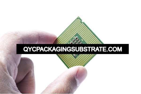
What is a ball grid array (BGA) packaging substrate?
Ball Grid Array Package Substrate Firm. the Package Substrate will be made with BT base, Showa Denko or Ajinomoto High speed materials.or other types high.
Ball grid array (BGA) packaging substrate is a common key component in PCB engineering, used to support and connect electronic devices. Different from traditional pin-type components, the BGA packaging substrate adopts a more advanced and compact design to meet the needs of modern electronic equipment for space utilization and electrical performance.
In the BGA package substrate, the balls welded to the bottom of the package form a two-dimensional array (Grid Array). These solder balls are used to connect the circuit between the package and the PCB board, replacing the traditional pin connection method. This design not only accommodates more connection points within the same area, but also transmits electrical signals more efficiently, improving electrical performance.
Ball Grid Array Package Substrate
In addition, because the solder balls are located at the bottom of the package, the size of the BGA package substrate in the vertical direction can be more compact, thereby achieving higher space utilization. This makes BGA packaging substrates particularly suitable for applications that have strict restrictions on PCB size, such as portable electronic devices and embedded systems.
In general, the BGA packaging substrate provides an efficient and reliable solution through its innovative design, which not only meets the connection density and performance requirements of modern electronic equipment, but also brings greater convenience to PCB engineers. Design flexibility and space advantages.
What types of ball grid array (BGA) packaging substrates are there?
Ball grid array (BGA) packaging substrates play an important role in modern electronic engineering, and the diversity of their types allows them to adapt to different application needs. Below we will introduce in detail several common types of BGA packaging substrates:
Organic substrates are typically made from organic materials such as epoxy or polyimide, which offer the advantages of lightweight, cost-effectiveness, and manufacturing flexibility. They are widely used in general electronic products such as smartphones, tablets, and computers.
Ceramic substrates use ceramic materials as their base and have excellent thermal conductivity and mechanical strength, making them suitable for high-power and high-frequency applications. Its stability and durability make it common in applications in demanding environments such as aerospace, medical equipment and military fields.
Metal core substrates are composed of a metal substrate (such as aluminum or copper) and an insulating layer, which has excellent heat dissipation performance and mechanical strength. They are commonly used in applications that require efficient heat dissipation and stability, such as LED lighting, automotive electronics, and industrial controls.
Flexible substrates are made of flexible materials, such as Mylar, that can be bent and folded, making them ideal for applications with tight spaces and curved designs. Flexible substrates are commonly used in portable devices, medical devices, and automotive interior electronic systems.
Each type of BGA packaging substrate has unique advantages and focuses on thermal management, electrical performance and mechanical strength to meet the needs of different industries and application fields. By selecting a BGA packaging substrate type that suits the needs of a specific project, electronic designers can ensure that their products achieve optimal levels of performance and reliability.
What are the advantages of using a ball grid array (BGA) packaging substrate?
The use of ball grid array (BGA) packaging substrates brings a series of significant advantages in modern PCB design, providing critical support for the performance and reliability of electronic devices. The following are several major advantages of BGA packaging substrates:
The BGA package substrate design can effectively improve heat dissipation capabilities and is especially suitable for high-power applications. Its unique structure and solder ball arrangement effectively conduct and disperse heat, effectively reducing component temperature and improving system stability and reliability.
BGA packaging substrates reduce the length and complexity of signal transmission paths, thereby reducing signal loss and the possibility of crosstalk. The solder ball connection method also provides a more stable and reliable electrical connection, helping to maintain signal integrity and ensure high performance of the system.
BGA packaging substrates have a more compact size than traditional packaging methods, allowing electronic devices to be lighter and smaller. This compact design helps improve the product’s appearance and portability, while providing more design flexibility to meet the needs of different scenarios.
Because solder ball connections provide a more robust and reliable connection method, BGA package substrates have excellent mechanical reliability. Compared with traditional pin connections, solder ball connections can better resist vibration and shock, thereby reducing the risk of components falling off or being damaged and extending the life of the device.
BGA packaging substrates achieve cost-efficiency by simplifying the assembly process and reducing material usage. The solder ball connection method simplifies the welding process and reduces manufacturing costs; the compact design reduces the space occupied and the amount of materials required, reducing material costs. This makes BGA packaging substrates an affordable and efficient option, especially for mass production and cost-sensitive projects.
In summary, BGA packaging substrates play a crucial role in the design and manufacturing of modern electronic devices due to their enhanced thermal dissipation capabilities, improved electrical integrity, compact size, excellent mechanical reliability and cost-effectiveness. important role.
Why Choose Ball Grid Array (BGA) Package Substrate?
In today’s fast-paced electronic design world, choosing the right packaging substrate is crucial. Compared with traditional pin-type PCBs, ball grid array (BGA) packaging substrates show obvious advantages, which are mainly reflected in the following aspects:
First of all, BGA packaging substrate has outstanding advantages in space efficiency. Due to its bottom solder ball design, BGA can achieve higher device density than traditional packaging methods, making the layout of components on the circuit board more compact, thus achieving space optimization in PCB design.
Secondly, the BGA packaging substrate performs well in maintaining signal integrity. The spherical solder joints welded on the bottom not only provide a shorter signal path, but also reduce the inductance and crosstalk of the circuit board, thereby ensuring the stability and reliability of signal transmission. This is particularly important for application scenarios with high-speed data transmission and frequent signal exchange.
In addition, BGA packaging substrates also have significant advantages in reliability. Compared with the traditional pin connection method, the solder ball soldered on the bottom can better disperse heat and improve the heat dissipation performance of the component. At the same time, the connection method of solder balls is also stronger and can resist mechanical vibration and impact, making electronic equipment more durable and reliable.
Finally, BGA packaging substrates can accommodate high-density interconnections and a variety of component types, providing more possibilities for modern electronic design. Whether in the fields of consumer electronics, automobiles, aerospace or industrial control, BGA packaging substrates have shown wide application prospects and become one of the first choices of electronic engineers.
In summary, based on its obvious advantages in space efficiency, signal integrity and reliability, as well as its applicability to a variety of application scenarios, ball grid array (BGA) packaging substrates have become one of the first choices in modern electronic design .
What is the manufacturing process of ball grid array (BGA) packaging substrate?
The manufacturing process of ball grid array (BGA) packaging substrates is a complex and precise process designed to ensure high quality and reliability of the final product. The following are the key steps of this manufacturing process:
The first step in manufacturing a BGA package substrate is to prepare the substrate. Typically, glass fiber reinforced organic substrates or ceramic substrates are used as substrates. These substrates must undergo rigorous inspection and processing to ensure that their flatness and surface quality meet manufacturing requirements.
Once the substrate is ready, the next steps involve stacking the layers onto the substrate. These layers include circuit layers, insulating layers, and metal layers, which are bonded together through lamination and thermocompression processes. The design of the layer stack must be carefully planned to ensure that the required signal and power transmission paths are achieved and that thermal management and electrical performance requirements are met.
In the BGA package substrate manufacturing process, solder ball connection is a crucial step. This involves adhering tiny solder balls to pads on the bottom of the substrate, which will be used to connect the packaged chips or other components. Solder ball connections usually use ball-shaped solder particles and are connected to the substrate pads through hot pressing or soldering processes to achieve electrical and mechanical connections.
The last critical step is surface treatment to ensure that the BGA packaging substrate has appropriate surface properties and corrosion protection. Surface treatments can include gold plating, tin plating, spraying or other types of surface treatments to provide a protective coating and improve soldering performance.
Each manufacturing step must be carefully designed and executed to ensure consistent quality and reliability of the BGA packaging substrate. Defects in any link may lead to failure or instability of the final product. Therefore, quality control and quality assurance during the manufacturing process are critical to ensure that each BGA package substrate meets the requirements of the final application.
What are the applications of ball grid array (BGA) packaging substrates?
Ball Grid Array (BGA) packaging substrates are used in a wide range of industries, and their versatility and reliability make them ideal for applications requiring high performance in challenging environments.
First of all, BGA packaging substrates play a key role in the field of consumer electronics. In electronic products such as smartphones, tablets, and laptops, BGA packaging substrates are widely used to integrate processors, memories, sensors, and other key components. Its compact size and high-density layout enable electronic devices to achieve higher performance and smaller size, meeting consumers’ needs for portability and efficiency.
Secondly, the automotive industry is also one of the important application areas of BGA packaging substrates. Modern cars are equipped with a large number of electronic control units (ECUs) for managing engines, safety systems, entertainment systems, etc. BGA packaging substrates play an important role in connecting and controlling various sensors, actuators and communication modules in automotive electronics. Its high reliability and vibration resistance enable it to operate stably in harsh vehicle working environments.
In addition, the aerospace field is also one of the important application fields of BGA packaging substrates. Aerospace equipment has extremely high requirements on performance, reliability and weight, and BGA packaging substrates are an ideal choice to meet these requirements. In aerospace, satellite, navigation systems and other equipment, BGA packaging substrates are widely used in data processing, communications, navigation and control systems to ensure efficient operation and long-term stability of the equipment.
Overall, BGA packaging substrates play an important role in various industries such as consumer electronics, automotive, and aerospace. Its versatility, high performance and reliability make it an indispensable part of modern electronic design, driving technological innovation and development in various industries.
Where can I find Ball Grid Array (BGA) packaging substrates?
When you need reliable Ball Grid Array (BGA) packaging substrates, you can rely on our company as your preferred supplier. As one of the trusted suppliers and manufacturers, we are committed to providing various types of BGA packaging substrates to meet the diverse needs of your projects.
Whether you are looking for a standard solution or require a custom design, we can meet your needs. Our company has rich experience and professional knowledge and can provide you with high-quality and reliable BGA packaging substrates to ensure the smooth progress of your project.
As one of the industry’s leading suppliers, we are committed to providing the highest quality services to electronic designers around the world. Our products comply with international standards and undergo strict quality control to ensure that each BGA packaging substrate meets the highest quality requirements.
Whether you are looking to purchase in bulk or order in small quantities, we are able to provide flexible solutions to meet your needs. Our customer service team is here to support you and resolve any questions and issues you may have.
In short, when you need a ball grid array (BGA) packaging substrate, you may wish to consider choosing our company as your partner. We will do our best to provide you with the highest quality products and services to meet your needs and achieve your project goals.
How much is the quotation for ball grid array (BGA) packaging substrate?
When determining the quote for a ball grid array (BGA) packaging substrate, several factors need to be considered, such as type, size and quantity. Different types of BGA packaging substrates have different cost structures. For example, organic substrates may be more economical than ceramic substrates, but ceramic substrates may have better performance in high-temperature environments. Size is also an important factor, with larger substrates likely requiring more materials and processing steps and therefore a corresponding increase in price. In addition, the quantity ordered will also have an impact on the quotation. Generally speaking, bulk ordering can enjoy a lower unit price.
In order to get a competitive price, it is recommended to obtain quotes from multiple suppliers and compare them. This way you can understand the price levels on the market and choose the most attractive supplier. In addition to price, factors such as the supplier’s reputation, delivery time, after-sales service, etc. should also be considered to ensure comprehensive advantages.
When evaluating an offer, a variety of factors should be considered, not just the price itself. The ultimate goal is to select the most cost-effective supplier that can meet quality and performance requirements while delivering the right solution within your budget.
Frequently Asked Questions (FAQs)
What are the typical applications of BGA package substrates?
BGA package substrates find extensive use in various applications across industries such as consumer electronics, automotive electronics, telecommunications, aerospace, and medical devices. Their versatility and reliability make them suitable for high-performance and compact electronic systems.
Are BGA package substrates environmentally friendly?
BGA package substrates can be manufactured using materials and processes that adhere to environmental regulations and standards. Additionally, their compact design and efficient thermal management contribute to energy savings and environmental sustainability in electronic systems.
How can I obtain quotes for BGA package substrates?
Quotes for BGA package substrates can be obtained from reputable suppliers and manufacturers who specialize in electronic packaging solutions. Providing detailed specifications and requirements will help ensure accurate and competitive quotes for your project.
What are the common challenges associated with BGA package substrates?
Common challenges associated with BGA package substrates include ensuring proper solder ball attachment, managing thermal dissipation in high-power applications, and addressing potential reliability issues such as solder joint fatigue. Working closely with experienced design and manufacturing teams can help mitigate these challenges.
Can BGA package substrates be customized for specific project requirements?
Yes, BGA package substrates can be customized to meet specific project requirements in terms of size, shape, material properties, and electrical characteristics. Customization options allow for tailored solutions that optimize performance and reliability for diverse electronic applications.