 Professional Flip-Chip Packaging Substrate Supplier

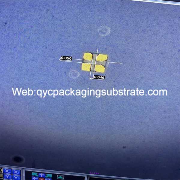
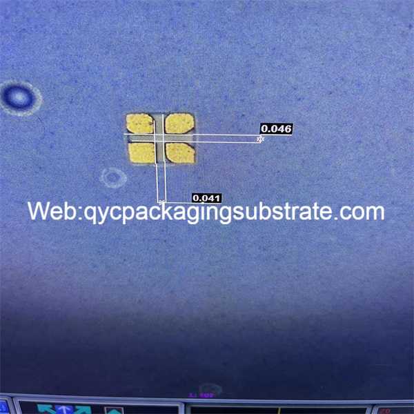
Ultra-Small Gap PCB
Ultra-Small Gap PCB manufacturing: Super small spacing with trace:41um/41um. and the best smllest via size are 50um. and ultrathin finished thicknees boards.
In the booming development of the electronic field, “Package Substrate” as a key component plays a vital role in electronic packaging. This component carries complex electronic devices, provides basic structural support and electrical connections, and is an integral part of modern electronic engineering.
“Package Substrate” can be understood as the cornerstone of electronic packaging. It provides a structurally complete and electrically connected platform for electronic components.
“Package Substrate” effectively supports these tiny and complex chips through its solid structure, ensuring that they can operate stably in different environments.
Secondly, as a medium for electrical connection, “Package Substrate” connects the chip to other electronic components through complex circuit wiring. This electrical connection is particularly important in high-frequency PCB engineering, especially in scenarios where ultra-small gaps and high-frequency transmission are required. In this field, the keyword “Ultra-small gap high frequency PCB” leads us to the next level of technological innovation.
The design of “Package Substrate” is not only about structure and connection, it also directly affects the performance and stability of the entire electronic system. When designing Ultra-Small Gap High Frequency PCB, engineers need to accurately consider the material selection, layer design, and electrical characteristics of the “Package Substrate” to ensure the reliability and stability of signal transmission under high-frequency conditions.
Overall, “Package Substrate” is a key technology in electronic packaging. It promotes continuous innovation in modern electronic engineering by providing structural support and electrical connections for chips. In the Ultra-Small Gap High Frequency PCB design that pursues ultra-small gaps and high-frequency transmission, the role of “Package Substrate” has become increasingly prominent, playing a key guiding role in the performance improvement and innovation of electronic equipment.
Ultra-small gap high frequency PCB
What is the function of Ultra-Small Gap High Frequency PCB?
In the field of electronic engineering, a new era of Ultra-Small Gap High Frequency PCB (Ultra-Small Gap High Frequency Printed Circuit Board) has arrived. These advanced PCBs are not only the cornerstone of electronic equipment, but also technological masterpieces in the field of high-frequency signal transmission. Let’s take a closer look at their core features and how they excel in high-frequency signal transmission with minimal signal loss.
The main function
The main functions of Ultra-Small Gap High Frequency PCB are multiple and exquisite. First, they are designed to support the transmission of high-frequency signals to meet the ever-increasing demands for data transmission rates and spectral efficiency of modern electronic devices. By using advanced materials and designs, these PCBs effectively reduce signal transmission losses and ensure signal clarity and stability.
Secondly, the design of Ultra-Small Gap High Frequency PCB focuses on reducing the gaps between electronic components, further reducing the signal transmission path and reducing the signal transmission time. This compact design helps reduce signal latency and improve circuit response speed, especially in time-sensitive applications such as communications and radar systems.
Application in high frequency signal transmission
These advanced PCBs play a key role in applications that require high precision and reliability. In the fields of medical equipment, satellite communications, radio frequency identification (RFID), and wireless communications, Ultra-Small Gap High Frequency PCB has become a key factor in promoting technological progress. They not only meet the needs of devices for high-frequency communication, but also shine in applications in microwave and millimeter wave bands.
In medical equipment, these PCBs ensure high-fidelity transmission of medical images and biological signals, providing doctors with more accurate diagnostic information. In satellite communications, they ensure fast transmission of data and highly reliable connections, supporting smooth long-distance communications. In the field of RFID and wireless communications, Ultra-Small Gap High Frequency PCB’s low signal loss and highly integrated design improve the performance and stability of wireless devices.
Importance and future prospects
The importance of Ultra-Small Gap High Frequency PCBs is that they push the forefront of electronic engineering and provide a solid foundation for technological innovation in different industries. With the rise of 5G and the Internet of Things, the demand for high-frequency communications continues to increase, and the application prospects of this kind of PCB are even broader.
In general, Ultra-Small Gap High Frequency PCB plays an indispensable role in electronic equipment with its excellent high-frequency signal transmission performance. Their design principles and material selection make them technological stars in modern electronic engineering, not only meeting current needs but also laying the foundation for future technological innovations.
What types of Ultra-Small Gap High Frequency PCB are there?
In the field of electronic engineering, Ultra-Small Gap High Frequency PCB is evolving at an impressive speed, and its diverse types provide professional solutions for different electronic design needs. Let’s take a deeper look at these types, each unique in meeting specific needs, from traditional substrate-like PCBs (SLP) to leading high-density interconnect (HDI) substrates.
Substrate-like PCBs (SLP)
Substrate-like PCBs, or SLP for short, represent a traditional and classic Ultra-Small Gap High Frequency PCB type. This type of PCB is known for its relatively thin substrate and excellent high-frequency performance. By cleverly integrating radio frequency components into the design, SLP-type PCBs can transmit high-frequency signals in ultra-small gaps, providing excellent performance for electronic devices.
Ultra-small gap high frequency PCB
High Density Interconnect (HDI) Substrate
High Density Interconnect (HDI) substrates represent a new generation of Ultra-Small Gap High Frequency PCBs, which are designed to minimize the gaps between components to increase signal transmission efficiency. Using fine lines and advanced stacking technology, HDI substrates accommodate more components in a relatively small space, making them ideal for high-frequency applications. Through clever lamination and embedded technology, HDI substrates can achieve compact layout of complex circuits and meet the continuous pursuit of high performance and miniaturization of modern electronic equipment.
A new generation of innovative Ultra-Small Gap High Frequency PCB
As technology relentlessly advances, a suite of innovative Ultra-Small Gap High-Frequency PCBs has emerged, catering to increasingly stringent application demands. These cutting-edge PCBs represent the synergy of advanced materials science and precision manufacturing technology, delivering heightened design flexibility and superior performance for high-frequency electronic devices.
Upon closer examination of these Ultra-Small Gap High-Frequency PCBs, it becomes evident that electronic engineering has achieved substantial progress in the relentless pursuit of devices that are smaller, lighter, and higher performing. Whether it’s the SLP, HDI substrate, or the latest generation of inventive PCBs, each contributes significantly to various domains, playing a crucial role and laying a robust technical foundation for the evolution of modern electronic equipment.
Engineers now have more choices and flexibility when selecting Ultra-Small Gap High Frequency PCBs for specific applications to meet the needs of different industries. This enables electronic devices to better adapt to increasingly complex and diverse communication and high-frequency application scenarios.
How is Ultra-Small Gap High Frequency PCB different from traditional PCB?
With the rapid development of electronic engineering, the difference between Ultra-Small Gap High Frequency PCB (Ultra-Small Gap High Frequency PCB) and traditional PCB has become increasingly prominent. From motherboard design to chip packaging technology, the differences between the two play a crucial role in shaping modern electronic devices.
Innovation in motherboard design
The motherboard design of traditional PCB often focuses on versatility and is oriented to various application scenarios. However, with the continuous advancement of technology, Ultra-Small Gap High Frequency PCB has focused its design on the transmission efficiency of ultra-small gap high-frequency signals. This customized design is more suitable for applications that have strict requirements on high-frequency response and precision, such as communication equipment and radio frequency modules.
Improved substrate utilization
Ultra-Small Gap High Frequency PCB has made significant progress in substrate utilization. Traditional PCBs are usually limited by line width and line spacing, while ultra-small gap high-frequency PCBs achieve a more compact layout through advanced high-density interconnect (HDI) technology. This means that more electronic components can be accommodated in a limited space, thereby increasing circuit density and performance.
Innovation in chip packaging technology
Chip packaging technology is a vital part of electronic equipment. Ultra-Small Gap High Frequency PCB uses advanced technologies such as improved semi-additive methods to achieve more precise and efficient chip packaging. This innovation not only improves the integration of components, but also optimizes the stability of signal transmission and is suitable for a wider range of high-frequency applications.
Overall, the evolutionary differences between Ultra-Small Gap High Frequency PCB and traditional PCB stem from the continuous optimization of high-frequency signal transmission and packaging technology.
What are the main structures and production technologies of Package Substrate?
In the continuous development of the electronic field, Ultra-Small Gap High Frequency PCB has become the focus of attention. Its complex structure and advanced production technology provide key support for the design of high-performance PCB. Let’s take a closer look at these amazing technologies and structures.
The construction of the Ultra-Small Gap High Frequency PCB is at the core of its high performance. First, they use advanced interconnect technology, which is reflected in improved high-density interconnect manufacturing technology.
Secondly, Ultra-Small Gap High Frequency PCB also adopts an innovative semi-additive method. This manufacturing technique allows for more detailed control by adding films layer by layer in the areas where they are needed, rather than over the entire substrate. This precise processing method helps achieve fine apertures and precision wires, providing PCBs with higher density and faster signal transmission speeds. The introduction of the semi-additive method further pushes the technological boundaries of PCB manufacturing, providing more flexible and reliable solutions for high-frequency applications.
Cutting edge of production technology
In the production process of Ultra-Small Gap High Frequency PCB, a series of cutting-edge technologies are also involved. This is critical to maintaining signal integrity in high frequency environments.
Secondly, advanced material selection is one of the keys to the success of Ultra-Small Gap High Frequency PCB. High-frequency applications have higher requirements on dielectric constant and loss factor, so the selection of materials is more challenging. By using optimized high-frequency materials, Ultra-Small Gap High Frequency PCB can achieve lower signal transmission losses, thereby improving performance.
The complex structure and advanced production technology of Ultra-Small Gap High Frequency PCB have jointly created its prominent position in the electronics field. From improved high-density interconnects to innovative semi-additive methods, the adoption of these technologies allows PCBs to adapt to the needs of increasingly complex electronic devices, enabling more compact, efficient designs. As technology continues to evolve, Ultra-Small Gap High Frequency PCB will continue to push the frontiers of electronic engineering and lay a solid foundation for future innovation.
Ultra-Small Gap High Frequency PCB FAQs
When discussing Ultra-Small Gap High Frequency PCBs, we inevitably run into some common questions. Here are answers to these questions, covering the technology’s application areas, manufacturing challenges, and industry trends.
In which applications are Ultra-Small Gap High Frequency PCB widely used?
The Ultra-Small Gap High-Frequency PCB is predominantly deployed in sectors demanding stringent specifications for high-frequency signal transmission. Its applications span a diverse range, encompassing communication equipment, radio frequency (RF) modules, radar systems, and medical devices. Renowned for its exceptional signal transmission performance, this PCB excels in scenarios that necessitate high precision and unwavering reliability.
What are the challenges in manufacturing Ultra-Small Gap High Frequency PCBs?
Manufacturing Ultra-Small Gap High Frequency PCBs requires meeting multiple challenges. One of them is precision manufacturing requirements, as these PCBs often require extremely small gaps and highly precise inter-layer connections. In addition, material selection, process control and cost-effectiveness are also important factors to consider during the manufacturing process. Technicians must consider these factors to ensure the production of Ultra-Small Gap High Frequency PCBs with excellent performance.
What are the industry trends for Ultra-Small Gap High Frequency PCB?
Currently, Ultra-Small Gap High Frequency PCB is experiencing rapid development and is expected to continue to lead technological innovation in the future.
Is Ultra-Small Gap High Frequency PCB suitable for mass production?
While there are some challenges associated with manufacturing Ultra-Small Gap High Frequency PCBs, production efficiency and scalability are increasing as technology advances. The introduction of advanced manufacturing technology and precision process control has made Ultra-Small Gap High Frequency PCB more feasible in mass production, providing the possibility to meet growing market demand.
Answering these frequently asked questions provides insight into the key applications, manufacturing challenges, and future trends of Ultra-Small Gap High Frequency PCBs. Continuous evolution in this field will bring more innovation opportunities to electronic engineers and manufacturers, pushing the performance of electronic devices at high frequencies to new heights.