 Professional Flip-Chip Packaging Substrate Supplier

ABF Substrate Vendors. FCBGA Package Substrate were made with ABF(Ajinomoto) core materials. they are: GX92R,GXT31R2, GZ41R2H, GL102R8HF and others. or Showa Denko Series material. they are MCL-E-705G, MCL-E-770G, MECL-E-700G, MCL-E-795G and others. you also can use BT base. Rogers base and other types conventional material.
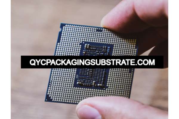
FCBGA Package Substrate (Flip Chip Ball Grid Array Package Substrate) is an advanced packaging technology that has attracted much attention in modern PCB engineering. It uses an innovative layout method of flipping the chip and is connected to the motherboard through a precisely arranged ball grid array to provide excellent performance and reliability for electronic devices.
In this advanced packaging technology, the FCBGA packaging substrate enables a more compact design and higher integration by flipping the chip to the back. In this way, the heat dissipation effect of the packaging substrate is maximized, and the reliability of the electrical connection is also significantly improved.
The core of this packaging technology lies in flipping the way the chip is laid out. By mounting the chip upside down, the chip’s connection points are directly exposed on the surface of the packaging substrate. The chip is then connected to the motherboard through a precisely arranged ball grid array. The design of this ball grid array not only provides a high degree of electrical connection density, but also provides an excellent channel for signal transmission, thereby achieving high-speed, high-frequency data transmission.
This advanced design of FCBGA Package Substrate brings multiple benefits. First, by directly connecting the chip to the motherboard, the signal transmission path is shorter, thereby reducing signal delay and improving the system’s response speed. Secondly, the structure of the ball grid array not only increases the connection density, but also enhances the reliability of electrical connections and reduces resistance and inductance.
When manufacturing FCBGA packaging substrates, process technology becomes particularly important. Including improved HDI manufacturing technology and semi-additive methods play a key role in this. The introduction of these technologies has made the manufacturing of packaging substrates more precise and controllable, ensuring high-quality production.
In general, FCBGA Package Substrate, as an advanced packaging technology, plays an important role in PCB engineering. Its flipped chip layout and precision connection of the ball grid array provide innovative solutions for improving the performance and ensuring reliability of electronic equipment. In the ever-evolving electronics field, FCBGA packaging substrates will continue to promote technological progress and provide strong support for future innovation.
What are the functions of FCBGA Package Substrate?
FCBGA (Flip-Chip Ball Grid Array) packaging substrate is an advanced and high-profile packaging technology. Its unique design and structure make it play a key role in the field of modern PCB engineering. When we deeply understand the functions of FCBGA Package Substrate, we found that it not only provides mechanical support for integrated circuits, but also ensures the performance and reliability of electronic devices through two main functions: electrical connection reliability and effective heat dissipation. Effect.
First of all, the FCBGA packaging substrate ensures highly reliable connections between electronic components through its precise electrical connection structure. This is accomplished by flipping the chip over and soldering it to a ball grid array on the substrate. This design helps minimize the resistance and inductance of signal transmission, thereby improving the performance of the circuit. In addition, because FCBGA uses spherical pins, it has significant advantages in the transmission speed and stability of electrical signals compared to traditional packaging methods.
FCBGA package Substrate
Secondly, FCBGA packaging substrate is known for its superior heat dissipation performance. In modern electronic devices, the heat generated by high power density and high performance chips is a problem that cannot be ignored. FCBGA quickly transfers heat to the surrounding environment through effective heat dissipation design to ensure that the chip can maintain an appropriate temperature during operation. This design helps prevent the chip from overheating and improves system stability and longevity.
The keyword “Flip-Chip Ball Grid Array” (FCBGA) plays a key role in this context. This advanced packaging technology achieves the dual functions of electrical connection and heat dissipation through the structure of spherical pins and flipped chips. In terms of electrical connection, the design of the ball grid array minimizes the resistance and inductance of signal transmission and improves circuit performance; in terms of heat dissipation, the carefully designed heat dissipation structure ensures that the chip can maintain a suitable operating temperature while maintaining high performance.
Overall, FCBGA packaging substrates provide critical support for modern electronic devices through their excellent electrical connections and heat dissipation properties. The wide application of this technology makes FCBGA packaging substrate an indispensable choice in high-density and high-performance applications. Its function is not only to connect the chip and the motherboard, but also to provide a solid foundation for the reliability and performance of electronic equipment.
What are the different types of FCBGA Package Substrate?
As an advanced technology, FCBGA (Flip-Chip Ball Grid Array) packaging substrate has derived many types during its development process. The differences between these types are mainly reflected in layers, materials and connection technologies. This diversity enables FCBGA to meet the specific needs of different application fields for high frequency, high-speed transmission and low power consumption.
First, the FCBGA packaging substrate presents a multi-level design in terms of hierarchical structure. This multi-level structure allows the substrate to accommodate more components and improves integration. For highly complex electronic equipment, this hierarchical structure design enables FCBGA to meet the needs of dense circuit layout and ensure the accuracy and stability of signal transmission.
Secondly, FCBGA packaging substrates use different materials to adapt to different working environments and application needs. High-performance electronic equipment has extremely high requirements for heat dissipation performance, so some FCBGA packaging substrates use advanced heat dissipation materials to ensure that the chip can maintain an appropriate temperature when operating under high loads. At the same time, high temperature resistant and low loss materials are also widely used to improve the stability and reliability of the overall system.
In terms of connection technology, FCBGA packaging substrates show flexibility and diversity. For high-frequency and high-speed transmission applications, some FCBGAs adopt advanced micro-wire connection technology to reduce resistance and inductance during signal transmission and improve signal quality. At the same time, for low-power applications, some FCBGA packaging substrates use low-power materials and advanced power management technology to reduce power consumption while meeting performance requirements.
In general, the various types of FCBGA packaging substrates provide the possibility for flexible application in different application scenarios. Whether in communication equipment, computer hardware or embedded systems, FCBGA packaging substrates are able to provide devices with excellent performance and reliability through their multi-layered structure, diverse material selection and flexible connection technology according to specific needs. This makes the FCBGA packaging substrate an indispensable key component in the design of today’s high-performance electronic equipment.
What is the relationship between FCBGA Package Substrate and IC packaging?
In the vast world of chip packaging technology, FCBGA packaging substrates have emerged and play a pivotal role. This advanced packaging technology is not only a key component of today’s IC design, but also has a special status in many aspects, providing a solid foundation for high performance and high reliability of electronic devices.
First of all, the importance of FCBGA packaging substrate in IC packaging technology is self-evident. Its unique flip chip layout and ball grid array connection design allows the chip to be more compactly integrated inside the package, effectively reducing the size of the package. This compactness is crucial to the pursuit of smaller size and lighter weight in modern electronic devices, and FCBGA packaging substrates play an irreplaceable role in this field.
Secondly, the FCBGA package substrate performs well in terms of electrical connections. In the tide of IC packaging technology, FCBGA packaging substrate has become one of the first choices to achieve these requirements.
In the entire IC packaging technology, FCBGA packaging substrate also has a special status in terms of maintainability and repairability. Its structural design makes the chip easier to repair and replace, which is particularly important in the context of rapidly developing technology and market changes. This special status ensures the sustainability of the equipment and extends its life in the market.
Overall, FCBGA packaging substrate not only plays an important role in IC packaging technology, but also has a special status in many aspects of chip packaging technology. Its compact design, excellent electrical connections, efficient heat dissipation and good maintainability make it an indispensable part of the design of modern electronic equipment. With the continuous advancement of technology, FCBGA packaging substrate will continue to lead the development trend of IC packaging technology and lay a more solid foundation for the future of electronic equipment.
What is the difference between FCBGA Package Substrate and traditional PCB?
When comparing FCBGA package substrates and traditional printed circuit boards (PCBs), we can observe significant differences in their structures, manufacturing processes, and applications. Below is a detailed exploration of the differences between PWBs and PCBs, motherboards, substrates, and similar substrate PCBs (SLP) and HDI substrates.
The difference between PWBs and PCBs
Traditional PCB (Printed Circuit Board) usually adopts a layer-by-layer structure, in which electronic components are connected through copper foil. However, the FCBGA packaging substrate uses advanced flip chip technology and is connected to the motherboard through a ball grid array, making the layout of electronic components more compact, thus improving the integration and performance of the circuit.
Similarities and differences between motherboards
In motherboard design, the FCBGA packaging substrate provides a more direct connection method for the chip, making signal transmission faster and more stable. This direct connection helps reduce signal transmission delay and improves the response speed of the entire system, which is especially important for high-performance applications.
The difference between substrates
The substrate design of FCBGA packaging substrates is usually more complex to accommodate advanced packaging technologies. Compared with traditional PCBs, substrates may contain more layers and more complex structures to support high-density layouts and more electronic components. This design makes the FCBGA package substrate more suitable for small devices and provides greater flexibility.
The difference between SLP and HDI substrates
In terms of substrate-like PCB (SLP) and high-density interconnect (HDI) substrates, FCBGA package substrates have higher integration and performance. SLP often uses advanced materials and manufacturing processes to make the substrate thinner and lighter while maintaining a high degree of reliability. The HDI substrate provides higher signal transmission rates and smaller component spacing through denser layout and fine line technology, thereby adapting to the demand for high performance.
In summary, the innovations in structure, manufacturing process and application of FCBGA packaging substrate compared to traditional PCB make it an advanced packaging technology that has attracted much attention in the current electronic field. Its unique design and performance advantages provide more possibilities for electronic devices in various fields and drive the entire industry forward.
What are the main structures and production technologies of FCBGA Package Substrate?
In modern PCB engineering, the structure and production technology of FCBGA (Flip-Chip Ball Grid Array) packaging substrate play a crucial role. Let’s delve deeper into this advanced technology, focusing on key aspects of its structure and production techniques, including improved HDI manufacturing technology and improved semi-additive methods.
Structure of FCBGA package substrate
The structure of the FCBGA package substrate is the cornerstone of its high performance and reliability. This packaging technology uses a flipped chip design that is connected to the motherboard through a ball grid array. Each ball grid is a tiny solder joint used to carry electrical signals and power. The advantage of this design is its compactness and high density, making the connection between the chip and the motherboard more compact and reliable.
In addition, the multi-layer structure of the FCBGA packaging substrate is its eye-catching feature. By using multi-layer stacking technology, more circuit components can be accommodated in a limited space, improving overall performance. The electrical connections between each layer are realized through advanced inner layer connection technology, which further improves the signal transmission speed and stability.
Production technology of FCBGA packaging substrate
HDI (High-Density Interconnect) manufacturing technology plays a key role in FCBGA packaging substrates. By using microscopic lines, apertures and stacked layers, HDI technology enables higher circuit density and shorter signal transmission paths. This helps reduce signal transmission delays and improves overall performance. In FCBGA, improved HDI manufacturing technology is used to further improve the integration and reliability of the packaging substrate by optimizing the design and production process.
Improved semi-additive method
The semi-additive method is an advanced manufacturing technology, especially suitable for the production of FCBGA packaging substrates. The method enables precise control of complex circuits by adding tiny conductive materials layer by layer on a substrate. The improved semi-additive method introduces more advanced materials and processes into the manufacturing process, improving manufacturing accuracy and efficiency. This helps ensure that all levels of the FCBGA packaging substrate can meet high performance and high reliability requirements.
By combining improved HDI manufacturing technology and semi-additive methods, FCBGA packaging substrates can achieve significant progress in miniaturization, high-density circuit layout, and high-performance requirements. These advanced production technologies make FCBGA a key technology in current PCB engineering, promoting the development and innovation of modern electronic equipment.
FCBGA Package Substrate FAQs
How is FCBGA Package Substrate different from other packaging technologies?
The FCBGA packaging substrate uses flipped chips and ball grid arrays to connect to the motherboard. Compared with traditional packaging technology, its main difference lies in the layout and connection methods. This design provides higher performance density and reliability and is particularly suitable for applications with high performance requirements.
What application fields is FCBGA Package Substrate suitable for?
FCBGA packaging substrates are widely used in fields that require high performance, high-density layout and good heat dissipation. Typical applications include high-performance computing, network equipment, communication systems, and other electronic equipment that require high stability and heat dissipation.
What is the manufacturing cost of FCBGA Package Substrate?
The cost of manufacturing FCBGA packaging substrates is relatively high, mainly determined by its advanced manufacturing technology and materials. However, these costs are generally considered a worthwhile investment given their superior performance in high-end applications.
What are the similarities and differences between FCBGA Package Substrate and HDI substrate?
HDI (High-Density Interconnect) substrate is a high-density interconnection technology, while FCBGA packaging substrate is a packaging technology. Although both involve high-density layout, HDI focuses more on circuit connections, while FCBGA focuses on chip packaging and connections.
What is the future development trend of FCBGA Package Substrate?
In the future, we can expect FCBGA packaging substrates to make breakthroughs in more fields, especially driven by emerging technologies such as artificial intelligence, the Internet of Things, and 5G communications. Its advanced performance and layout features will continue to provide critical support for innovation in electronic devices.
How to optimize the heat dissipation effect of FCBGA Package Substrate?
Optimizing the heat dissipation effect of the FCBGA package substrate can be achieved by improving the heat dissipation design, selecting high thermal conductivity materials, and effective heat dissipation structures. This helps ensure that the chip maintains the proper temperature while operating, improving system stability.