 Professional Flip-Chip Packaging Substrate Supplier

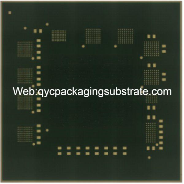
Package Substrate Prototype. We use advanced Msap and Sap technology to build the Substrates and Package Prototype , High multilayer interconnection substrates from 2 to 20 layers.
Package Substrate, as we can surmise from its name, is a key electronic element. But what is it? On the big stage of electronic engineering, Package Substrate is an integral part of carrying and connecting chip (IC) packages. It is made of non-conductive material and provides a stable support for the chip and a platform for connecting circuits.
So, what is the specific positioning and role of Pack age Substrate in electronic engineering? More than a simple support structure, it is a component that plays a key role mechanically, electrically, and thermally. Through internal conductive lines, Package Substrate achieves precise connection between the chip and external circuits, providing a solid foundation for the stability and performance of the entire system.
By deeply understanding the nature and role of Package Substrate, we can better apply it in electronic design and manufacturing and bring out its potential advantages.
What are the magical features of Package Substrate?
Have you ever thought about what kind of magical element Package Substrate is? As an indispensable item in electronic engineering, Package Substrate is not only a support platform for ICs, but also undertakes key mechanical support, electrical connections and heat dissipation tasks. As the solid foundation of the chip, it not only closely connects the IC to the external circuit through delicate conductive lines, but also provides solid support in the mechanical structure.
Mechanical support
Package Substrate plays a vital role in mechanical support. It is designed to hold the chip securely and withstand physical stress from the external environment. This ensures that the chip works safely and reliably in a variety of applications, whether it’s bumps in a mobile device or vibration in an industrial environment.
Electrical connections
As a key component of electronic systems, Package Substrate plays an important role in electrical connections. It enables efficient communication between the IC and external circuits through a sophisticated network of wires. This connection must not only ensure stable signal transmission, but also adapt to different electrical requirements to provide balanced and coordinated electrical performance for the entire system.
Heat dissipation
Thermal dissipation is another unique feature of Package Substrate. In modern electronic devices, the high performance of chips is often accompanied by the generation of heat. Package Substrate helps effectively conduct and disperse the heat generated by the chip by designing a unique heat dissipation structure, ensuring that the chip maintains a stable temperature under high load.
Through these critical tasks, Package Substrate becomes an irreplaceable element in electronic engineering, providing a solid foundation for overall system reliability and performance.
Package Substrate
Different types of Package Substrate, do you know?
When we explored Package Substrate in depth, we found that it is not static, but covers multiple types. This leads us to ask: What does diversity in Package Substrate actually mean?
The Diversity of Package Substrate: A Wonderful Fusion of Materials and Structures
In PCB engineering, Package Substrate is not a backwater, but shows diversified characteristics. The diversity of this element is mainly reflected in the different classifications of its materials and structures.
Material classification
First, let us focus on the material classification of Package Substrate. Film-based, ceramic-based and organic-based are some of the main types. These materials play a key role in the manufacturing process of Package Substrate, determining its physical properties and electrical characteristics.
Film-based Package Substrate: uses film as the main support material. This type of Package Substrate is usually lightweight and flexible and suitable for applications that have strict weight and size requirements, such as mobile devices.
Ceramic-based Package Substrate: Using ceramics as the main construction material. Ceramic-based Package Substrate has excellent heat dissipation performance and mechanical strength, so it is often used in high-power and high-frequency electronic equipment.
Organic Package Substrate: uses organic materials, such as resin. This type generally has lower manufacturing costs and better processing properties, making it suitable for mass production and cost-sensitive applications.
Structural classification
Secondly, we need to understand the structural classification of Package Substrate. Different structural designs have a profound impact on the performance and stability of electronic devices.
Multi-layer structure: By stacking multiple layers, more complex circuit designs and layouts can be achieved. This structure is very common in high-density integrated circuit applications, providing more connection paths for electronic devices.
Rigid-flexible structure: Combining rigid and flexible materials allows Package Substrate to strike a balance between electrical performance and mechanical strength. This structure is often used in electronic products that require folding or curved designs.
By understanding the diversity of Package Substrate, we can better choose the type suitable for specific applications and optimize the design of electronic devices. In this diverse world, PCB engineers need to continue to learn and innovate to adapt to the needs of different types of Package Substrate and contribute to the progress of the electronics industry.
By delving into the different types of Package Substrate, we not only expand our understanding of PCB engineering, but also explore broader possibilities in the design and manufacturing of electronic devices. This gives us a deeper understanding of the application of this key element.
What is the relationship between Package Substrate and IC packaging?
When we delve into the Package Substrate in PCB engineering, we inevitably touch on its vital role in the field of chip packaging. Package Substrate plays an irreplaceable role in this field, providing support and connections for chips, and plays a key role in electronic devices through its special design.
In the vast world of chip packaging, Package Substrate is given multiple tasks. First, it provides mechanical support to protect the chip inside from the outside environment. This kind of mechanical support is not only a simple physical protection, but also creates a stable environment for the normal operation of the chip. Secondly, Package Substrate achieves a tight connection between the chip and external circuits through its complex circuit connections. This electrical connection is not just a simple conduction, but also a key channel for information transmission and control.
In the classification of chip packaging technology, the diversity of Package Substrate cannot be ignored. It can be based on different materials, such as film-based, ceramic-based and organic-based Package Substrate. These types of choices directly affect the performance and applicable scenarios of the package. Thin-film-based Package Substrate is usually thin and flexible and suitable for applications with limited space, while ceramic-based Package Substrate is more suitable for applications in high-temperature environments.
Furthermore, Package Substrate and IC packaging technology complement each other. Chip packaging technology covers various forms from single-chip packaging to multi-chip packaging. Single-chip packaging usually uses traditional BGA (Ball Grid Array) packaging technology, while multi-chip packaging may involve 3D IC packaging and System-in-Package (SiP) technology. Package Substrate serves as a key medium in these packaging technologies, enabling efficient connection and collaborative work between chips.
In general, Package Substrate’s position in the field of chip packaging is not unimportant. It provides a solid foundation for the stability, reliability and performance of electronic devices through unique design and material selection. For PCB engineers, a deep understanding of the key role of Package Substrate in chip packaging will bring more innovation and advantages to the design and manufacturing process.
The competition between Package Substrate and traditional PCB
You may have wondered, what is the difference between Package Substrate and traditional PCB? In the vast field of electronic engineering, how are motherboard, Substrate, and HDI Substrate related to each other?
Similarities and differences between Package Substrate and traditional PCB
First, let’s explore the similarities and differences between Package Substrate and traditional PCB. As a special electronic component, one of the main differences of Package Substrate lies in its material and structure. Compared with traditional PCB, Package Substrate uses more types of substrates, such as film substrates, ceramic substrates and organic substrates. This enables Package Substrate to provide a more flexible and adaptable solution when hosting and connecting chips.
The evolution of motherboards: Traditional PCB vs. Package Substrate
The motherboard is the core of electronic equipment, and Package Substrate plays an increasingly important role in this field. Compared with traditional PCB, the application of Package Substrate on the motherboard shows higher integration and performance. Its unique structure and diverse material selection allow Package Substrate to occupy a place in compact designs and high-efficiency electronic devices.
The connection between Substrate and electronic engineering
The concept of Substrate is widely used in electronic engineering, and Package Substrate is its evolution and extension. Substrate is a substrate. Package Substrate enables chips to work together in complex electronic systems through its powerful mechanical support and electrical connection functions. This allows electronic engineers to better handle highly integrated electronic components.
HDI Substrate: The future of high-density interconnect
In terms of high-density interconnection (HDI), Package Substrate performs better than traditional PCB. Innovations in its structure and manufacturing technology enable HDI Substrate to accommodate more components in a smaller space, improving the performance and reliability of electronic devices.
By comparing Package Substrate with traditional PCB, we see the evolution in electronic engineering. The rise of Package Substrate not only expands design possibilities, but also provides new ways to improve the performance of electronic devices. In the fields of motherboard, Substrate and HDI Substrate, Package Substrate is gradually becoming the new darling of electronic engineering, paving the way for future innovation.
What is the essence of structure and production technology?
Are you curious about what is unique about Package Substrate’s structure and production technology in PCB engineering? As a PCB engineer with 10 years of work experience, let us delve into the inner mysteries of Package Substrate. From the unique features of the construction to the innovative techniques used in the manufacturing process, let’s find out.
The uniqueness of the structure
The structural design of Package Substrate is crucial. First, we need to understand how it is built. What are the structural differences between film-based, ceramic-based and organic-based Package Substrates? How do these differences affect its application in electronic engineering?
Thin film-based Package Substrate usually uses soft materials, and its flexibility makes it suitable for some scenarios that require higher mechanical properties. Ceramic-based Package Substrate is known for its high strength and thermal conductivity, and is often used in applications with stringent stability requirements. In contrast, organic-based Package Substrate focuses on lightweight and cost-effectiveness.
In addition, in the structural design, Package Substrate also needs to consider how to better combine with the chip and package to achieve the best electrical connection and heat dissipation effect. This has important implications for the different types of IC packaging technologies.
Innovative technologies in the manufacturing process
After understanding the structure of Package Substrate in depth, let us turn to its production technology. What innovative technologies are used in the manufacturing process to ensure high-quality Package Substrate?
In the current field of PCB engineering, the manufacturing of Package Substrate is no longer a simple processing process. Among them, improved HDI manufacturing technology is an eye-catching innovation. This technology enables more layers and smaller line widths, thereby improving board integration and performance. This innovative technology provides greater flexibility in the design of Package Substrate compared to traditional methods.
Another emerging manufacturing technology is the modified semi-additive method. This approach reduces scrap during manufacturing and improves process controllability by gradually building up layers of copper foil onto the substrate, rather than applying it all at once.
By continuously introducing such innovative technologies, the manufacturing of Package Substrate has gradually achieved higher efficiency and more advanced performance, providing strong support for the development of electronic products.
By in-depth understanding of the structure and production technology of Package Substrate, we can more fully grasp the status of this key element in PCB engineering..
Frequently Asked Questions (FAQs)
You may have a preliminary understanding of Package Substrate, but are your questions about it really satisfied? Let’s dig deeper together and answer a series of Frequently Asked Questions (FAQs) about Package Substrate to help readers more fully understand this key element.
Q: What element in electronic engineering is Package Substrate?
A: Package Substrate is an electronic component that plays a key role in PCB engineering. It is usually composed of non-conductive materials and is used to support and connect chip packages.
How is Package Substrate different from PCB?
Q: What are the essential differences between PCB and Package Substrate?
A: PCB (Printed Circuit Board) is mainly used to support and connect various electronic components, while Package Substrate is more focused on providing mechanical support, electrical connections and heat dissipation functions for chips.
What are the common Package Substrate types?
Q: What are the different types of Package Substrate?
A: Common Package Substrate types include film base, ceramic base and organic base. Each type has unique characteristics and is suitable for different application scenarios.
What is the role of Package Substrate in IC packaging?
Q: What role does Package Substrate play in IC packaging?
A: Package Substrate plays a key role in providing mechanical support, electrical connection and heat dissipation in IC packaging to ensure that the chip can operate normally.
What is the connection between HDI Substrate and Package Substrate?
Q:What is the connection between HDI Substrate and Package Substrate?
A:HDI Substrate is an evolved form of Package Substrate, using high-density interconnection technology to provide a more compact layout and higher performance for electronic components.
What innovative technologies are involved in Package Substrate’s manufacturing process?
Q: What innovative technologies are used in the manufacturing process of Package Substrate?
A: In the process of manufacturing Package Substrate, new manufacturing technologies such as improved HDI manufacturing technology and semi-additive method are introduced to improve production efficiency and product quality.
By addressing these commonly asked questions, our aim is to equip readers with a thorough grasp of the significance and wide-ranging applications of Package Substrate in electronic engineering. This indispensable element assumes a non-negotiable role in contemporary electronic design and manufacturing, laying a firm groundwork for enhancing the performance of diverse electronic devices.
Summarize
We first explained how Package Substrate is an indispensable element supporting IC packaging. It not only provides mechanical support, but also plays a vital role in electrical connection and heat dissipation. By learning the different types of Package Substrate, such as film base, ceramic base and organic base, we have a more comprehensive understanding of the characteristics and application scenarios of these elements.
We further discussed the close relationship between Package Substrate and IC packaging. In chip packaging technology, Package Substrate plays a key role, and its type and structure have a profound impact on all aspects of chip packaging. Through these discussions, we revealed the strategic position of Package Substrate in the entire electronic engineering.
Comparing Package Substrate and traditional PCB, we discovered the differences and connections between them. Whether it is used in motherboard design or in the field of emerging technologies such as Substrate-like PCB (SLP) and HDI Substrate, Package Substrate has demonstrated its unique value. This comparison allows us to better understand the application of Package Substrate in different electronic devices.
Finally, we gained an in-depth understanding of the main structure and production technology of Package Substrate. This includes its complex structure and the improved technologies involved, such as improved HDI manufacturing technology and semi-additive methods. This in-depth understanding helps engineers better select and apply Package Substrate, thereby improving the efficiency and performance of electronic design and manufacturing.
With a comprehensive understanding of this key element, we believe readers will be more confident in applying Package Substrate in their engineering practices. As a PCB engineer, having an in-depth understanding and flexible application of Package Substrate will bring greater advantages to your electronic design and manufacturing. This is not only a mastery of technology, but also a boost to future innovation. I hope this article can open the door to knowledge about Package Substrate for you and provide new inspiration for your career.